
If you’ve been around long enough, you’ll know there’s a long history of advances in materials science that get blown far out of proportion by both the technical and the popular media. Most of the recent ones seem to center on the chemistry of carbon, particularly graphene and nanotubes. Head back a little in time and superconductors were all the rage, and before that it was advanced ceramics, semiconductors, and synthetic diamonds. There’s always some new miracle material to be breathlessly and endlessly reported on by the media, with hopeful tales of how one or the other will be our salvation from <insert catastrophe du jour here>.
While there’s no denying that each of these materials has led to huge advancements in science, industry, and the quality of life for billions, the development cycle from lab to commercialization is generally a tad slower than the press would have one believe. And so when a new material starts to gain traction in the headlines, as perovskites have recently, we feel like it’s a good opportunity to take a close look, to try to smooth out the ups and downs of the hype curve and manage expectations.
Mind the Band Gap
To the extent that you’ve heard about perovskites – and you probably have, with coverage right here on these pages and a full Amp Hour podcast devoted to them – you’ve probably got the impression that they’re some newly discovered material that can be used to build solar cells that are better than the current crop of silicon photovoltaics. There’s a lot more to perovskites than PV, though, and the chemistry behind them is pretty interesting too.
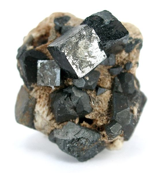
To start with, perovskite – note the singular – is a mineral, calcium titanate (CaTiO₃), first discovered in the Ural mountains in the late 19th-century and named after famed Russian mineralogist Lev Perovski. Naturally occurring perovskite deposits are found all over the world, and the mineral is mined commercially.
Perovskites, on the other hand, are natural and synthetic compounds that match the crystal structure of natural perovskite. The general form of perovskites is ABC₃, where C is usually oxygen and A and B are positively charged ions, or cations. A is generally an alkaline or rare-earth metal, while B is usually one of the metals from the transition series on the periodic table. Some synthetic perovskites even substitute organic cations for the inorganic metal, resulting in hybrid perovskites with interesting and useful properties ranging from superconductivity to optoelectronics.
The reason that perovskites have so much promise as photovoltaics is that they are much better at absorbing light than silicon, thanks to the fact that perovskites have a direct band gap, rather than silicon’s indirect band gap. The band gap of a material refers to the energy needed to move electrons around in it, and indirect band gap materials have to shuttle electrons around in a two-step process. The practical effect of this means that indirect band gap materials need to be thicker to absorb enough light to work. A silicon layer 200 microns thick is needed to absorb the same amount of energy as a half-micron layer of a hybrid perovskite such as a methylammonium lead trihalide (CH₃NH₃PbX₃, where X is usually iodine or bromine). What’s more, the band gap of hybrid perovskites can be tweaked to cover more of the spectrum by fiddling with the ratio of halides, as shown in the featured image above.
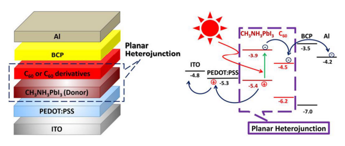
fullerene-based hybrid solar cells
Another selling point of hybrid perovskites is that can be made into aqueous solutions, which can then be applied to a substrate such as glass using very simple techniques like vapor deposition or spin-coating. There’s even work going on with printing perovskites using modified ink-jet printers. Contrast these processes with the laborious methods of silicon solar cell production, which basically require most of the trappings of a semiconductor fab, and you can see that the excitement about perovskite solar cells (PSCs) is justified.
Perovskites are not the be-all and end-all of solar cell technology, of course. There are significant problems, including lower efficiency than silicon cells. That’s likely a temporary problem, though; whereas silicon PVs have taken almost 70 years to get from 6% efficiency to the current 27% efficiency of commercial cells, PSCs are already at 23%, and they’ve only been in development since 2009. With more work, perovskite efficiency could eclipse silicon PVs and approach the theoretical maximum of 31%.
The real drawback for PSCs is engineering them to stand up to weathering; the water-solubility that makes hybrid perovskites so easy to work with also makes it tough to moisture-proof PSCs. UV degradation of the dyes is a problem, too – organic compounds are famously labile under UV radiation, and layers that can filter out the UV reliably without blocking other wavelengths need to be applied over the perovskite layer.
Sensors for X-Ray
The potential boost in efficiency and decrease in costs make it a good bet that the engineering problems surrounding PSCs will be addressed and full commercialization will begin. But turning sunlight into energy is far from the only trick that perovskites can perform, and might not even be their most lucrative application. Medical imaging, particularly with X-rays, is poised to benefit greatly from perovskite-based sensors.
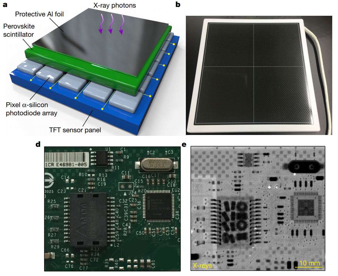
Being just another wavelength of light, X-rays interact with perovskites similarly, converting them to electric charges that can be sensed directly. This differs from the majority of current X-ray sensors used for digital radiography, which are indirect sensors – a plate covered with a compound that emits light when struck by X-rays, known as a scintillator, is sandwiched to a standard charge-coupled device (CCD), which picks up the light and creates a digital representation of the differential penetration of tissues by the X-rays. This has the benefit of being very sensitive and reducing the dose of X-ray necessary to produce an image, but at the cost of reduced resolution since light from the scintillator grains spreads out before striking the CCD detector.
A direct sensor, on the other hand, converts the incident X-rays directly to electric charges, greatly increasing the resolution that can be achieved. But conventional semiconductor direct X-ray sensors, which typically use selenium, suffer from the same problem that silicon does when used as a solar cell – it doesn’t absorb electromagnetic radiation very well. That makes selenium detectors slow to acquire an image, requiring a higher X-ray dose. Perovskite direct sensors, though, absorb much better and result in far better resolution sensors that require much lower doses.
Many of the same hurdles facing the commercialization of perovskite in solar cells remain for X-ray sensors. But the multi-billion dollar medical imaging industry may well have the upper hand in getting perovskites to market first. It’s far easier to protect a perovskite X-ray sensor from the moisture and rough handling associated with patient care than it is to engineer PSCs to withstand the years of sleeting ultraviolet rays and wind-driven rain that any practical solar array has to deal with.
That said, what’s learned by the medical imaging applications for perovskites will no doubt drive the development of PSCs, and our guess is that perovskites will be a household word within the next five years or so.
[Featured image source: National University of Singapore]


But not as a replacement for the CCD itself.
Talking about the thickness of photocells has me thinking.
What if a cell was made extra thick and the connecting wires were not just wires but ribbons standing on edge? I’m thinking only the top so much of the cell would actually generate electricity because photons would only penetrate so far. But what about aging. Would the inner, inactive portion of the cell be protected from aging?
Would this result in a cell where after so many years of degradation one only need to go over it with a floor sander, remove the top x-microns perhaps paint on a transparent protective coding and then have a brand new fully-functional cell again?
That wont work. Solar cells consist of multiple layers. It’s more like a transistor you have N-doped and P-doped layers. If you start shaving or sanding off layers you would be permanently damaging the cell. Furthermore even if you did stack the cells consistently shaving off 200microns is probably not worth the cost to invest in new higher efficiency panels by the time your existing cell would benefit from such a treatment. There’s also the upfront cost of investing in what is effectively 2 solar cells to future proof yourself against an efficiency loss of X%. It’s a good thought but not very practical.
The magic happens at the junction between N-type and P-type semiconductors. So if you sand away the top, you’ll remove the N-type completely and the junction with it.
A very thick layer may not work well for both solar cells and the x-ray detector because the photo excited electrical charges have a limited diffusion length. If the layer is too thick, excited charges would recombine before reaching the contact layers to be collected, and then we would not get electrical power output from the solar cells or signal output from the detectors.
How does one play the space from a financial prospective? Are there any publicly traded companies? Thnx
nanosolar cells are foil printed and they are allready available, and if the following prize is valid ist only 17 cent / Wp, thats insane.
https://www.secondsol.com/de/anzeige/15576/nanosolar/nanosolar/utility-panel-160w
First, a bit sus as there’s no picture of the panel…
Second, the panel is 1.9 meters by 1.3 meters…. at 160W for a panel bigger than my house’s doors, that’s quite low…
I had a “100W” (probably 50W) silicon one smaller than that, used it with a mains PSU for 15-300V in and 5V 4A out.
I’ve now got a fold up panel with a similar surface area of material (lesser Silicon in sun though) ,
It’s an all-powers 21W USB (2x 2.1A out) charging solar panel… mine’s the 4X panel version, the current ones are only 3X panel meaning the total of the 4x panels must be capable of up to about 30W (estimate, likely higher) in great conditions if I were to modify it to house another DC-DC, it can even be fully loaded in cloudy conditions.
That’s roughly 800mm by 30mm of panel area…
Everyone likes to point out the “feat” in terms of the rapid efficiency increase with perovskites. It’s like the last 70-80 years never even happened.
I’ve seen many “miracle solar panel” stuff over the past decade alone where the panels are on par with those in cheap “solar calculators”…. the ones with a real panel that is…
When scaled up in size to charge batteries, I got one for cheap from maplin’s “discount” bin (years before they shut) and got a Si panel at the same size…
I was able to pull more power from the silicon one.
Also, the “demos” of such “miracle panels” proved iffy… or… showed underwhelming results and “just needs more research to hit predicted efficiencies” (I’ve heard that phrase plenty of times… like, free-energy, solar roads, plastic-from-air, etc… lol)
Perovskite has a different crystallographic structure that scientists and engineers are trying to take advantage of. The device physics of a how a solar cell operates isn’t changing so much. Perovskites have seen stellar leaps in efficiency because of all of the built up knowledge. You can change the crystal structure, but you still have the same functions in a device.
I am surprised if this has not been featured on Hackaday before: https://www.pvlighthouse.com.au/
This as well: https://www.pvlighthouse.com.au/cms/lectures/altermatt/principle
Instead of a water based solution why not an alcohol or ammonia based solution? Coat, slide into a low pressure chamber to make the volatiles evaportate faster and to recover them for re-use. Then spray on a clear urethane paint that’s formulated to only block UV light.
Why don’t you just make solar panel paint if you need help with this I would be happy to
OK, so I paint perovskites on my electric car, put on a UV opaque clear coat and I can drive forever?
If you manage 4 square meters of 25% efficient solar cells, that’s about 1 kW or 1.3 horsepower. So you can drive at maybe 10 mph if the sun is shining, you don’t have a headwind, and you don’t need to drive up even a shallow incline.
A gallon of gasoline is about 36 kWh, and an ICE might be 25% efficient. If your electric car has batteries that can store the energy from the cells without losses, you should be able to get the performance and distance of an ICE car using a little less than 1 gallon/day.
Jep, do-able, not so nice in winter, but in summer perfect.
https://www.youtube.com/watch?time_continue=81&v=fgjwjFLOIlc
Notice the lead-acid battery hanging under the frame. It’s not running off of the solar panels directly, because in one of the shots it was shown to be drawing over 500 Watts, and that panel isn’t large enough to make 500 Watts. It’s barely 200 Watts maximum pointed randomly like that.
they mention its a 3kW system so that itty bitty solar panel would do sweet FA as far as providing running power. At best it would give a top up if it was parked all day.
Well my car gets 40 rods to the hogshead so…
So where’s the catch? Mining it causes childbirth defects?
The main problem is actually the “lead” in this kind of materials. It will be difficult to reach mainstream applications…