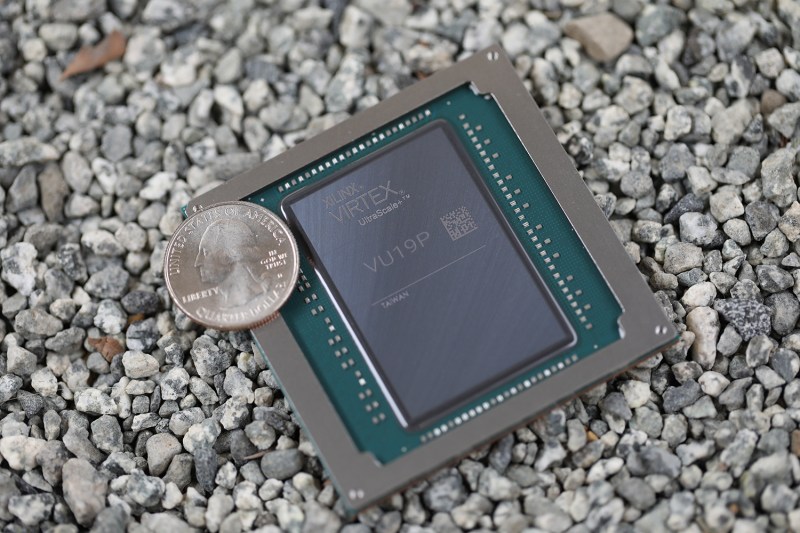
Xilinx recently announced the Virtex UltraScale+ VU19P FPGA. Of course, FPGA companies announce new chips every day. The reason this one caught our attention is the size of it: nearly 9 million logic cells and 35 billion transistors on a chip! If that’s not enough there is also over 2,000 user I/Os including transceivers that can move around 4.5 Tb/s back and forth.
To put things in perspective, the previous record holder — the Virtex Ultrascale 440 — has 5.5 million logic cells and an old-fashioned Spartan 3 topped out at about 50,000 cells — the new chip has about 180 times that capacity. For the record, I’ve built entire 32-bit CPUs on smaller Spartans.
That led us to wonder? Who’s buying these things? When I first heard about it I guessed that the price would be astronomical, partly due to expense but also partly because the market for these has to be pretty small. The previous biggest Xilinx part is listed on DigKey who pegs the Ultrascale 440 (an XCVU440-2FLGA2892E) at a cost of $55,000 as a non-stocked item. Remember, that chip has just over half the logic cells of the VU19P.
Beyond Silicon Verification
The press release mentions companies like ARM using these devices to test new chip designs before tape out. That makes sense, but there aren’t many companies that need chips this big for that purpose. Massive parallel processing might make sense, too. However, I suspect there might be a third class of customer.
In computer security, there’s a term: script kiddie. These are people who use software written by someone else to hack into computers because they lack the ability to write it themselves. I think these new super-sized FPGAs might be catering to the FPGA kiddies — people who mostly use FPGAs to compose custom ICs from existing intellectual property (IP) that they buy or acquire from the vendor. Pulling in multiple different FPGA IP uses up logic cells fast. If you don’t want to spend the time writing your own modules, you’re likely to opt for spending more on larger hardware instead of rewriting the code to occupy fewer resources.
Not that there’s anything wrong with that, the process of writing and testing these blocks of logic is a long and expensive one. Among many advantages of FPGAs is the ability to leap forward on the shoulders of tried and tested IP. The analog is using ICs to build circuits versus using discrete components for everything. Maybe the field has grown to the point that vendors should divide up the way they classify these parts. An FPGA is for traditional logic and a FRIC (Field Reconfigurable Integrated Circuit) is more a palette for IP. Then again, the parts are the same either way, I suppose.
Blame Your Tools
The tools, though, ought to be very different. The push with modern tools is to make logic synthesis, IP composition, and firmware development for processors all in one place. I’m not sure that makes as much sense as it seems on first blush. After all, if I’m building a DSP processing chain, I might not care about coding firmware for some embedded processor I’m not using. Conversely, if I’m programming some ARM core, it might not matter to me to be able to create a lot of logic. Sure, some people will blend all of these things together, but I’d bet that’s the exception and not the rule.
If that’s true, perhaps we really do need different tools for each type of FPGA user. I agree, of course, that it doesn’t have to be an either/or proposition. You might use an ARM processor along with some custom Verilog and a few pieces of IP.
Still, what would you use a 9 million cell FPGA for? If not parallel processing or extreme IP composition, how would you manage the complexity of something so large? Granted, with this price tag I think it’ll be a long time before we see any projects for it on our tip line. If you do happen to have access to one of these, please do something at least a little bit ridiculous with it and send us a link!
Learn More
You may not be able to configure 9 million gates, but you can learn about FPGAs in our bootcamp. Only one part of the series is specific to the Lattice Icestick — the $5 chip on that board has around 1,200 lookup tables and you can bet they are probably less capable per cell than the Virtex part. If you want to try putting an ARM CPU on a more reasonably priced part, there’s always this.


Probably has a few military customers as well who want to process camera data.
I was wondering about using for data mining all the communications or telemetry traffic in the World, or whatever jurisdiction, with whatever the AI or automated process is.
or wideband RF data
Brian knows things !! LOL
Working on this FPGA currently. Wideband RF Processing.
How wide a band ? :-)
Al – meanwhile back on planet Earth, the Lattice ICE 40 HX 4K is actually an 8K part knobbled by Lattice’s proprietary tool chain. You can buy them from Mouser for about $6.30 in 1 off – and they are still available in a home-solderable TQFP-144 package. With a cheap 10×10 cm board from China, and Clifford Wolf’s Project IceStorm OpenSource toolchain – you can get started with FPGAs for well under $20
The problem with FPGAs getting more accessible is that they’re getting harder to find an excuse to avoid. Soon I’ll have to pick one up and make it do my bidding. Hopefully not too soon…
How long until these replies are filled with “could available this with an Arduino!”
I can see it now. SCRATCH-HDL for KIDS!
Absolutely there are better FPGA based products for Makers / Hackers to tinker with or build systems upon. This VU19P is a Cargo Ship in comparison to the tiniest, entry level ICs you’re referring to, which would be more like kayaks.
I’d recommend Pynq or Ultra96 types of modules for the hobbyists. This is a chip for chipmakers, not tikerers… Though I’d love to see what some Makers could do with it.
Sweet! I want to put one on my bicycle for playing music and Galileo. Will it run Linux or do I have to use micro-python?
I hope they have an easy samples program!
_o/ need some at work for pre-silicon validation
Yes please. Still cheaper than an emulator
Perfect! Emulation & Prototyping is a primary target market for the big boys.
FPGA computer chipsets.
CUDA compiled to FPGA.
https://dl.acm.org/citation.cfm?id=2847344
FPGA based VMs.
http://docplayer.net/4589040-Fpga-based-system-virtual-machines.html
FPGA prototyping.
http://semiengineering.com/fpga-prototyping-gains-ground/
Here is an example of a device likely to use these chips for large scale IP composition: https://www.synopsys.com/verification/prototyping/haps.html
The market is definitely there for it.
There’s a couple minute YouTube video that talks about the target applications. Primarily Emulation, Prototyping (which you pointed to), Test (ala PCIe protocol analyzer), and Measurement.
https://www.youtube.com/watch?v=dyJnYdPdrac
Think about network content analysis in realtime
This is the right answer – it’s a huge market. I work with someone who came from this industry, as an FPGA engineer, and they do indeed use these high-end parts.
Agreed, though some of the regular or other Virtex UltraScale+ devices are generally more well suited to that. Often the NW analysis guys don’t need the most giant FPGA, they just need the latest, greatest high performance ones with the latest , fastest transceivers (like 58G serial for 400Gbps Ethernet). Or maybe the ones w/ a bunch of HBM DRAM integrated with the FPGA fabric (logic).
I am really wondering why Xilinx is not officially fixing it’s ISE support for Windows 10? Instead they are giving a Virtualbox heavy bundle of 14.7 On top of a Linux distro. This is terribly slow on a windows 10 with even moderately latest i7 8th gen which can clock upto 4+ GHz with 12 logical cores.
I recently got my hands on a spartan 6 Papilio pro board. Then I realised Xilinx is not interested in further support for these devices and recommending to move to latest series and these devices are only supported on their older ISE 14.7 and not in the Vivado.
But luckily I found some smarts guys fixed this issues by just renaming few DLL files or so to make it work perfectly in windows 10.
So why can’t Xilinx officially do it ? Why giving such a big headache of a Virtualbox disk disk image on top of Linux to make it difficult for someone to use on Windows 10 device? :)
?
May be because they want people to forget the Spartan 6 and move to their latest devices? I guess.
Look at this video for more details:
https://youtu.be/VMEIPCjqinA
Just renaming a DLL makes it work perfectly with windows 10 :) If a user can fix it, why still Xilinx not publishing it in their official website? Why still Ise 14.7 in Virtualbox disk image with Linux distro for windows 10? May be if Xilinx is seeing this, please update it because it will be a huge help for spartan6 and 6- users.
Initially I downloaded a huge bundle of a Virtualbox image disk from Xilinx official website a month ago to try Spartan 6. It was terrible and slow and I got fed-up with it. Then I found this trick to make it work normally on windows 10 device :) Thanks to whoever did this initially. Someone else did this initially before this guy but this person’s video seems more useful for anyone to imitate it to make the 14.7 windows build to work seemelessly.
It sounds like you make your life harder by not using open-source software.
I’ve heard tell of places on this planet that actually forces a person to use closed-source, proprietary software (gasp!) in exchange for something called a paycheck. I know, it sounds strange, but I think there are more of them than one could imagine.
I am very much new to FPGA. Could you suggest me some good free software alternative to develop on a spartan 6?
Please suggest some alternative free software to develop on spartan 6. I am new to FPGA even though I am having a decent experience on hardware and firmware.
Bruce : it sounds like you’re pretty new to the FPGA world ;-)
Proprietary FPGA tools running on proprietary OS has always been the plague of the field, since the very first FPGA came along.
Ah the glorious times when you needed a full HP Apollo workstation with the token-ring server loaded with full Mentor Graphics licenses to compile an antifuse FPGA with barely 1K cells…
For more than 20 years, users have fought every fight to get Actel, Altera, Xilinx, Lattice, and all the other contenders, so their tool would finally work on Linux. And even when they tried, the failed, miserably, making their huuuuuuuuuuuge bloatware even more miserable, rendering the proprietary platform “almost desirable”.
20 long years… and i’m still forced to maintain a laptop with Windose because those who decide are the finance&marketing people, not the engineers.
Oh and now they all outsource to underpaid incompetent Indian subcontractors, adding even more misery to the misery.
And I don’t even mention other roadblocks like the setup and expiry of the licenses…
Don’t get me started.
When a good working Terminator will be put in service, I suspect the engenners will send it to “test” its capabilities on marketing and financial people…
These are the kinds of decisions made by the business end.
I’m just guessing, but I’d bet that they believe that the likely customer base for FPGAs in excess of $50k wouldn’t think twice about buying a latest, greatest workstation for the development of the end product.
But for a beginner still Spartan 6 is a good choice and lot of resources are available online.
It is like, still people suggest to buy Arduino Nano and try to program it directly using avr-gcc by reading datasheet of atmega328p by skipping the Arduino wrapper and ide environment for a better understanding and learning of MCU even though AVRs are too old compared to latest stm8s and similar much cheaper latest devices. :)
I believe, Xilinx may be purposefully doing it to force people to use new latest FPGA instead of the old-school but powerfull spartan 6. Old is gold and sad about it. :(
Nope. I don’t think they *can* do it. I’m not even sure if they have any ISE developers around anymore.
ISE was entirely dropped and replaced with the newer IDE, Vivado, which actually originates from a completely separate company’s tool (Hier Design’s PlanAhead – they were acquired by Xilinx back in 2004, PlanAhead was a “separate development environment” in ISE after a while, and then PlanAhead evolved into Vivado.
The reason Vivado only supports the newer FPGA designs is that the 7-series FPGAs are much more unified than previous generations, so instead of supporting many different architectures that need different optimizations, Vivado just supports one.
Which, of course, means that Spartan-6 users get totally screwed, since the S6 was the last new chip family Xilinx put out before the 7-series stuff came out.
Any recommendations for beginners?
The irony is that the Plan Ahead is the software module inside ISE that won’t run in in 10 x64. The fix was to rename the x86 dll to run it in x86 code.
That’s only one of the problems (and you can fix it by just passing a ‘force 32-bit mode’ flag to it). The main problem is actually an ISE library (libPortability.dll).
Xilinx *does* actually have instructions to run ISE on Win8/Win10 here (which I’ve done personally, so I can say that it works):
https://www.xilinx.com/support/answers/62380.html
They just don’t “officially support” it, because they don’t “officially support” ISE at all anymore.
You’re probably right, Vinod. A Spartan 6 is _plenty_ for getting started. But Xilinx isn’t going to put R&D money into making “old” products work, especially if it’s incompatible with their current mainstream.
It would be super useful to have the S6s in the open toolchain, and this is known. https://github.com/SymbiFlow/ideas/issues/10 Just nobody has done it yet.
There are also chips like the Lattice ECP5 that would make a good S6 replacement for many purposes and for which there’s already an open-source flow. That’s where I’d put my money now, if buying new.
If you just want to hack on an old S6 board, or one embedded in a machine you care about, that may mean trying to find a way to make ISE work for you. Or get to work hacking the Spartan 6 into the open flow. :)
I recently stared playing with FPGA (1 month back) and I am having a spartan6 papilio Pro board. I hope not needed to upgrade :)
I don’t think they really care about new spartan-6 designs at this point. The new stuff has been Vivado for many years. New big volume users will probably be on spartan 7 or artix, so they sell chips for exisitng SP-6 design ins, and keep ISE on life support with VM.
Windows is a legacy OS, a computing pariah who’s direct ancestor is the ugly bastard child of CP/M, VMS and Xenix… why should a company like Xilinx waste money supporting it?
Lol… more wisdom from the peanut gallery. Windows isn’t going anywhere.
So maybe *this* will be the year Linux takes over the desktop? lol.. and no, OSX has never and will never go above 10% market share.
What do you mean windos isnt ging anywhere? Iets been ging all over the place in the last few years. Its the reason of this complaint, the software does t work with win10 anymore (officially). While backwards compatibility is a thing normally, it often happens that its not. So yeah its all over the place.
We now have open hw CPUs, I guess open hw FPGAs would be next.
Because of they are market leader. They can tell you what you must do, they don’t listen at your needs. They don’t reply to mail request not care you at all. Because they are market leader… And as*hole, too.
If only everything were free…
And who could possibly need more than 640k in a PC? (As someone once said.) It’ll fill up alright, and the price will come down, and one day it, or something similar, will be run-of-the-mill.
That disk holds 360K? Wow! That 3-pack (Elephant memory systems– “An elephant never forgets!”) should last me forever!
I’ve spent some time at work opening dead network switches and looked at some pretty serious linecards for juniper routers and various CMTS brands.
You usually find some pretty hefty FPGAs in all of that gear, I was kinda surprised when I saw a reminder that you had to make sure the FPGA on a switch was running the correct version before running a firmware upgrade.
It does make a lot of sense being able to upgrade the hardware with new fixes and features through software while its humming away in a dark room somewhere.
This is the kind of hardware that is probably barely hitting double digit thousands of units produced. The only ones buying them are big telecom/ISP folks. The hardware demands high prices due to the markets they are aimed at which means just loading the board up with FPGAs is cheaper than spinning custom ASICs, not to mention it gives the hardware longer lifetimes in the telecom/ISP’s racks because as major flaws might be found that would mean chucking the whole thing in the bin, instead a “firmware” upgrade can be issued to reconfigure the FPGAs to fix the issues, or to even make custom one off hardware designs for the providers if their pockets are deep enough.
Possibly, although one wonders if the same effect will happen to hardware that is currently happening to software, and that’s releasing beta, this and that, and fixing it down the line (if). Instead of putting the effort in up-front ensuring a good design, that doesn’t need as much correcting later.
Totally! The AI / ML guys basically need this. If they make or buy an ASIC, they’re looking at a 3 year cycle from concept commit to first working silicon. AI / ML algorithms change drastically in just one year. So, the ASIC will be 2 years out of date by the time it’s in the lab. FPGAs are adaptable by their very nature, so play well in technologies that are still rapidly evolving.
A lot of market for this sort of thing is systems-level integration. You’ve got a product that will implement as much of the software stack in hardware as possible, and you want it to run for 10+ years, complete with firmware upgrades that add new features. There are some network vendors, for instance, who implemented most of their processing stack on FPGAs. The platforms built on FPGAs were able to add new features for years, while still implementing the features in hardware. There were military systems that did the same thing, using FPGAs to implement as much of the stack as possible, allowing upgrades over time.
I also suspect that a lot of these will end up in FPGA value add network interfaces for servers and switches in the low-latency trading market or big data market.
Maybe it’ll help jump start the open-hardware movement.
at long last… but I won’t hold my breath.
That’s what I was thinking too. Hopefully we build IP repositories for FPGAs that work like OSS IP does now. We have some interesting cores being designed but we will need interconnects, buses, peripheral controllers, and lots of supporting hardware to get to full open hardware based systems that can compete with PCs.
OSS and FPGAs could even lead to some interesting scenarios like an FPGA on an input port with a sort of bootstrap channel that lets a peripheral configure the interface dynamically.
But this will also bring new challenges in security and verification too. How do we prevent something from injecting some code that implants something potentially nasty in the ‘hardware’?
Need some Open Chequebook (TM) as the bleeding edge chips cost way more than the ”3 months salary” of the diamond industry. :P
One place I worked for used to write their own CAD, assemble their PCB and even had a fab because at the time what was on the market wasn’t good enough. The newer products used less and less of their own ASIC and move towards FPGA. The last project I was working on was down to 1 of our own ASIC with half dozen op ended FPGA at the time.
With FPGA, there is the economies of scale as the upfront cost of keeping up with the process node has been increasing exponentially as you are fighting physics. FPGA vendors let their customers share the R&D for getting chips fab, verified without the complex and cost of making their own ASIC. If you are using FPGA, all you need to retarget your design for the higher densities/speeds offered by the new devices.
These days only really big guys have the deep pockets of chasing process nodes to make their own ASIC.
Even the really big guys who are developing their own ASIC use FPGA’s to model at least parts of them. I know because I work for one and that’s what we do all the time. We already have much of the chip characterized before it goes out for fab.
Right. I heard one tagline from the launch press coverage that calls VU19P “The Chipmakers Chip”
Chipmakers who make chips of any large (revenue) significance need the most massive FPGA available to do what you’re talking about. They’ve got Nx$100M at risk.
The IRS probably took this as a shortcut.
Entire dead system architectures reimplemented in FPGA.
A “COBOL Processing Unit”
This is totally the wrong way to think about this.
The VU19P is just the logic and IO optimized version of the UltraScale+ Virtex family. It has nowhere near the most onboard RAM (same amount of UltraRAM as the VU3P, the smallest one, and same amount of block RAM as the VU9P), nowhere near the most onboard DSPs (barely more than the VU5P, the second-smallest one) and nowhere near the most transceivers (again, same as the VU5P/VU7P) or transceiver bandwidth.
With that many I/Os (and there are many use cases for a high-IO FPGA: extremely high-channel test and measurement, for instance), the die needs to be pretty big, and so obviously you just stuff the rest with logic since it’s easy. Plus the logic helps because with that big a die, there’s a hefty interconnect cost just getting data across the chip, so you’re probably going to want to keep the usage low.
The only reason Xilinx is making a “BIGGEST FPGA EVER” announcement is because long ago, FPGAs were nothing *but* logic, and so every time you made the biggest one, it was a big deal.
But the high cost for this FPGA isn’t really *that* big a deal: it’s almost certainly going to be cheaper than using 2 smaller VUP chips if you need that many I/Os.
I think so too. It’s probably a bit like with VLSI’s vs23s010: “We got a bunch of ram on this serial chip. But as it’s a serial chip, we have some pins left. And some real-estate on the die as well. Any good ideas? Ah yeah, let’s put a video display controller on it as well!”. :+)
I love it when they do these kinds of things.
They’ve been doing *something* like this for a while, but the UltraScale family is where it became really obvious that they’ll make a single IO-heavy FPGA (with the obviously stupid amount of logic because the die itself is so huge) and everyone else is going to be stuck at around ~600-800 I/Os, but have a lot more features.
My guess is that the high I/O market is shrinking, collapsing the number of high I/O family members to 1, and in the case of the VU19P, also collapsing it to only one package as well. The interesting thing is that apparently that market doesn’t have a huge need for DSPs, because although the DSP count did grow from the VU440, it didn’t grow nearly as much as the other members in the family. That tells you something about the market.
crypto mining , instagram face recognition , IA , big brother cameras and so many possible apps …
crypto mining is now in the realm of ASICs.
FPGA and GPUs are out of the speed/power league for a long time now.
Some coins are designed with the ability to change the mining algorithm, making ASIC development especially risky. And some others – like Curecoin and Foldingcoin – are specifically designed to run well on GPUs and there’s basically no gain making an ASIC to mine those.
That is definitely not true.
Not.
” but there aren’t many companies that need chips this big for that purpose”
GPU manufacturers. AMD, nVidia, Intel.
There is a huge market out there outside of tradition hardware – medical, military, telecom. Big companies like Google, Amazon, financial companies etc. for market that don’t have much to do with hardware ended up making their own chips or use FPGA to gain an edge on data processing or AI.
Just guessing here, but a product like this will often show up before the original purpose is declassified or breaks out from the IP constraints of the university that needed this thing.
I wonder if, much like the TCP offload card, there are many operations that consume processor time that end up being deterministic and could be removed from the primary processor if you had a large dynamic FPGA. Evaluate the ins and outs for a while and basically use the compression string table equivalent in processing. Review the cache for biggest wins, add those to the FPGA and then reroute those to the FPGA as they go by with a return back to the cache with a passthrough instruction.
Also, one could emulate not only the processor in an FPGA that big, but a board manufacturer and and peripheral makers could also emulate the north bridge and south bridge to create a rig that can test drivers for multiple disparate hardware specs before the physical boards roll off the line.
Also, I am totally out of my depth on this, but as we come up against physical constraints imposed by historical architecture there will need to be dramatic out of the box thinking, and a chip that big makes a playground big enough to fail fast, break things, and iterate through crazy ideas that might work without crystallizing it into hardware.
This is really just the I/O (and logic) optimized version for the UltraScale+ family.
It’s not that the “previous biggest FPGA” (the VU440) wasn’t “big” enough, it’s that it’s an UltraScale chip, not an UltraScale+ chip.
So if you need a high I/O FPGA and need higher data-rate transceivers for instance (or you need the huge on-chip RAM the UltraScale+ chips provide, you need this chip. Doesn’t matter that the logic count is so much larger, it’s the only one available. The cost probably isn’t going to be much different than the ~$50K VU440 as well – in any case, it’s going to be way cheaper than the 2x UltraScale+ FPGAs you’d need instead of this chip.
Not to mention the UltraScale+ guys are higher performance too, of course.
A lot of these high end FPGAs end up on PCIe cards destined for datacenters. AWS has FPGA instances: https://aws.amazon.com/ec2/instance-types/f1/
So even if you don’t need the full chutzpah of the Ultrascale+, you can rent time on it. Same with the mega mega Tesla GPUs from NVIDIA — those can do GPU virtualization for multiple hosts.
The High Frequency Trading mob live in a strange world; they install transatlantic submarine cables and buy up the microwave telecom towers between New York and Chicago, all to save a few milliseconds communication latency.
They also put the entire software stack including *business rules* in hardware, e.g. “if share price increased by 10% in the last 5 minutes, then sell shares”.
Bingo. The market is much bigger than the author thinks. Xilinx is not losing money on this.
“Still, what would you use a 9 million cell FPGA for? If not parallel processing or extreme IP composition, how would you manage the complexity of something so large?”
Test equipment: Millimeter-wave 5G development, Electronic Warfare dev/test. DDS/AWG/VNA/VSA etc. A part like this is a god-send in these fields, and the customers have deeeep pockets.
Cellular industries are good ones for this kind of stuff, rather than buying all new cellular modems for cell towers every 5-10 years when a new G comes out, FPGA based equipment might be able to last though several generations, with a simple “firmware” update to the FPGAs in the radios to support the new standard, make the analog front ends modular that if and when needed they could be swapped out if the new standard demands it but leave the core digital DSP processing in place for a decade or two. This would mean just upgrading some analog front end cards every few years rather than throwing out whole racks full of equipment.
If you remember the good old days of dialup internet and the standard war between 56k x2 and 56k Flex with 33.6 modems that were being sold as being ready for a 56k future with a simple firmware update, you were probably basically dealing with dialup modems that had FPGA DSPs, They could be simply updated to the new 56k standard once the dust settled on the standard war.
Hah! THREE POSTS A CHARM. When are you going to FIX this horrible comment system HaD?
HaD uses automatic pre-censorship so whenever they troll their readers with controversial topics, they can flag users and certain words or language for pre-moderation and that way they can control the discourse. On one hand it’s keeping the trolls out, on the other it’s controlling exactly what people can say about their articles.
Previously they just let the buzz happen for a day or a week, and then went back to the comment sections to delete every comment they didn’t like — but that meant there was this gap where people could see the comments and that was just inconvenient.
This is my third reply that probably didn’t go through either.
You got away with this one.
I think there’s somewhere between “FPGA Kiddies” and ASIC/etc prototyping that is a niche for this strata of FPGA. It’s nice to prototype an ASIC in an FPGA where you have fabric (routing logic and logic cells especially) to spare. Your design will synthesize faster and with a higher fmax when the place-and-route doesn’t have to strain itself.
Another aspect is when you have multiple asynchronous transceivers, you need multiple PLL’s and associated clock routes to properly test an ASIC’s synchronization logics.
tl;dr It’s nice to not have to cram a large design into an FPGA when prototyping.
They’re for SoC validation. Plenty of smaller players are trying to bolt together the blocks created by the big boys.
I really don’t get the « script kiddies » analogy being used here🙄
Agreed. I’m trying to figure out of it’s an allusion to lazy designing where you rely on the excess system fabric to make up for lack of optimisation. I wouldn’t call using vendor IP lazy, rather, efficient.
Right, why re-invent the wheel?
Script Kiddies could come from the fact that the cutting edge emulation approaches may often use script based partitioning and massively build procedures to fill up hundreds of these devices at a time. For. One. Design.
Lol. I need this to flashing my LEDs.
With my luck, I’d connect power and ground backwards…
“What do you mean the I/Os aren’t 5V tolerant?!” (smoke)
I’d say if you’re buying individual FPGA ICs you’re buying more than one of them and not paying the ridiculously inflated prices Digikey lists. Most of the FPGAs listed in the $40K range have development boards available in the $3K range… If there wasn’t a substantial bulk discount it would be cheaper to buy a bunch of dev boards, desolder and reball the FPGAs
As several others have mentioned, the largest use-case for such FPGAs, by far, is in data centers. Microsoft, Amazon, and Google are gobbling them as fast as Xilinx and Intel (Altera) are able to produce them.
Microsoft has published several papers on using such FPGAs for ultra-fast network switching and routing in Azure data centers. The big 3 cloud players also use them for inference in certain kinds of AI applications.
Finally, both AWS and Azure provide FPGA instances. Even if it costs well north of $100k a pop to buy one, it’ll still be very cheap to use for a few hours a day on a cloud instance, probably under $3/hr (for comparison, you can get a 32 core, 256GB RAM instance for as little as $1.7/hr on Azure). At such a price, it’ll probably be cheaper to prototype on such a VM even if your project doesn’t need more than 100k gates. Heck, you could even throw together a proof of concept using said vendor IP, just to see if your idea makes sense.
One use case that came to mind immediately is large scale data acquisition and processing. Something like CERN’s LHC ATLAS experiment. It can generate upwards of a petabyte of data per second. An FPGA like this can preprocess and compress the data down to something more manageable for normal datacenter storage solutions.
I have built a simple pong clone on my spartan 3 and spartan 6 dev boards. I wonder how fancy a version of pong I could build using this monster of an FPGA? 😛
The Big Xilinx are used in the Gemini board of the SKA project developed by Astron.
Here is a design paper of it : https://www.researchgate.net/publication/316324649_Gemini_FPGA_Hardware_Platform_for_the_SKA_Low_Correlator_and_Beamformer
Think about compute acceleration applications – with decent DDR access you can have far better performance with such a device than any top notch GPU.
Is 8xDDR4 x72 ‘decent’?
“Who Could Possibly Need An FPGA With 9M Logic Cells And 35B Transistors?”
what a silly question, of course the answer is: US Army/Marine/Airforce/CIA/whatever-usa-military-or-intelligente-agency.
When it came out a hardware with some order of magnitude bigger that actual top level and that appear so powerfull to be unusefull, the US military are the natural first user (an usually, also the committer).
So, the quarter in the lead photo is not the price of the chip?
I guess so.
I’m currently designing a thermal management system for the Virtex Ultrascale+. I can assure you that there are plenty of people using these things and pushing them to their max. The FPGA alone is responsible for 80 Watts of heat dissipation in our application.
Incidentally the biggest snag with FPGAs is the hideously overcomplicated toolchain where the software costs 10,000* more than the chip(s).
Sure its possible to write your own which will eventually work but its cheaper to just pay the $$$$ and use theirs.
Plus the resulting config will fit in the cheaper chip and not waste power like some Eldritch abomination made in a shed using salvaged 1080Ti array running on liquid metal cooling. And when you want to change one parameter somewhere its relatively simple rather than a week long slog .
There’s a litany of sins hidden in many FPGA designs. Just as laywers are often paid by the word, I fear–so too–are many logic designers are paid by the gate.
I don’t know what your requirements are to hold the title of largest FPGA, but I think Intel has it right now.
https://blogs.intel.com/psg/intel-announces-intel-stratix-10-gx-10m-fpga-worlds-highest-capacity-with-10-2-million-logic-elements-targets-asic-prototyping-and-emulation-markets/
IXIA is a big user … they recently tossed out 100 pieces of a XCVU13P-2FHGB2104 … some of the parts in the XCVU13P series list for $88,766.64 on digikey! Ixia uses 8 at a time on some of their boards!
do some deep learning on it, would absolutely kick butt. Dont know why its not more commonplace. wierd.
Maybe because it’s extremely, ridiculously expensive ?