Most electronics we deal with day to day are comprised of circuit boards. No surprise there, right? But how do they work? This might seem like a simple question but we’ve all been in the place where those weird green or black sheets are little slices of magic. [Teddy Tablante] at Branch Eduction put together a lovingly crafted walkthrough flythrough video of how PCB(A)s work that’s definitely worth your time. 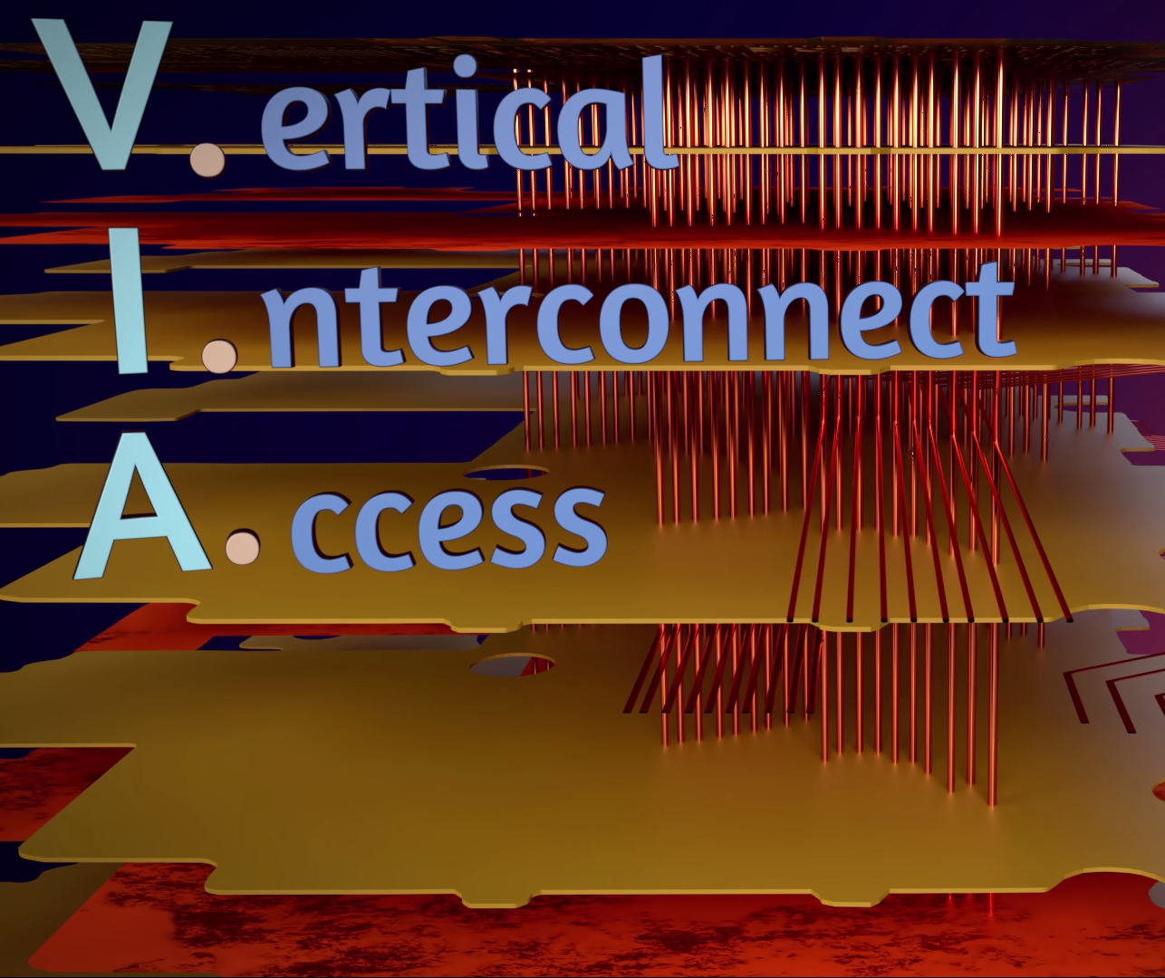
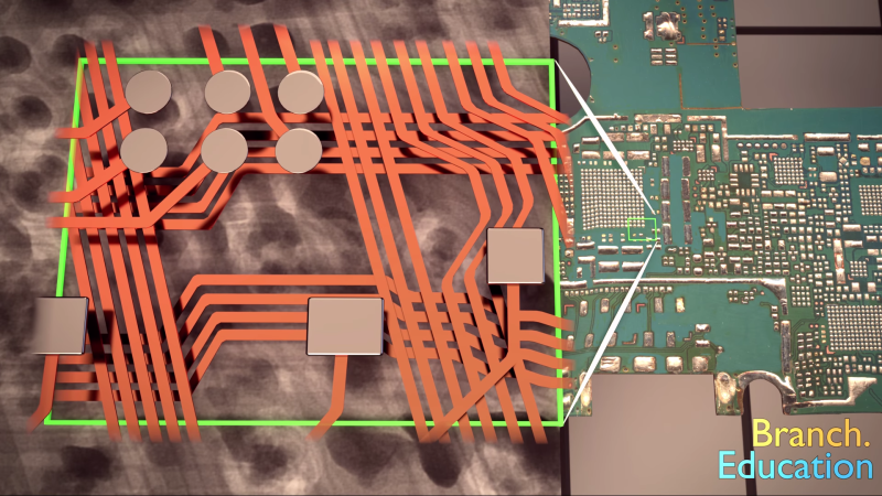
[Teddy]’s video focuses on unraveling the mysteries of the PCBA by peeling back the layers of a smartphone. Starting from the full assembly he separates components from circuit board and descends from there, highlighting the manufacturing methods and purpose behind what you see.
What really stands out here is the animation; at each step [Teddy] has modeled the relevant components and rendered them on the PCBA in 3D. Instead of relying solely on hard to understand blurry X-ray images and 2D scans of PCBAs he illustrates their relationships in space, an especially important element in understanding what’s going on underneath the solder mask. Even if you think you know it all we bet there’s a pearl of knowledge to discover; this writer learned that VIA is an acronym!
If you don’t like clicking links you can find the video embedded after the break. Credit to friend of the Hackaday [Mike Harrison] for acting as the best recommendation algorithm and finding this gem.


Via is not an acronym. It’s Latin for street or way.
This. But now that someone’s said that, the erroneous backronym will infect the internet in perpetuity.
It can be once it’s had it’s periods.
While you and I may have learned “via” as a word in common use, there are plenty of references (via Google)–recent and ancient–which seem to validate “vertical interconnect access” == “[VIA]” lending some credence to the author’s explanation of VIA as an acronym.
There’s enough patent database research links to support the belief that VIA is also an acronym, despite its otherwise useful translation from Latin. For example:
http://www.patbase.com/classSnapshot/public/?class=H05K3/4053&system=CPC
Hundreds of copper wires??
Missing just a few zeros there buddy.
Why not just say dozens or gross or great gross?
That’s a good question, how many wires would you say total are in that PCB? How long would the netlist be?
I do not see why it could not have be an apronym (An acronym that is an existing word.) by design.
It’s possible, but I have know about PCB vias for decades and never heard that it was an acronym until today.
same, been doing PCB’s for decades, never heard it as an acronym until this video
Dubious acronyms are funny. A few years ago, a neighbor tried to tell me CCCP stood for Central Committee of the Communist Party, apparently not questioning why the Soviet Union would name itself with Latin words/letters vs. it’s own Cyrillic.
The Access in the supposed via acronym seems pretty contrived. Interconnect would say all that needs to be said for connecting layers, and it’s not like vias are commonly used as test points or something.
How do you access a buried via?
What if your board is designed to sit at a different angle? Do they become hias if they happen to be horizontal?
Here are some other acronyms from the 1970s or so… EPROM, CPU, PIO, VIA (but not the kind that’s part of a… PCB. Spot the difference between these and the way we write via. What about the way we say them, See Pee You but not Vee Eye Ay.
Even though I was quite neutral about ‘via’ being an acronym, this solid logic convinced me that it cannot be true.
The science behind the making of that video would be interesting enough.
I was not planning on watching the video, but your comment peaked my interest. That video was very well animated.
Says in the comments he used Blender and about 115 hours of work.
The article reminded me of Mike milling away at PCB layers:
https://www.youtube.com/watch?v=RHqN6CTOdzA
Been in electronics manufacturing for 28 years at 4 different companies, 2 of which were CMs with dozens of customers and this is the first I have heard via being used as an acronym. In general though, most of the video is a good explanation for those that are non-technical. There are a few other comments in the video that are not quite accurate, but for this purpose, they are irrelevant. In general, the video overall is well done for explaining the complexities of a PCBA.
If you have access to gerber data for a design, check out ZofzPCB’s 3D gerber viewer. You can get better 3D views of a board design than the animations shown in this video. It is extremely helpful when needing to “dive in” to a board design for analysis purposes. Check out the demo video on their home page: https://www.zofzpcb.com/
How many meters of wire are in the various chips on the board? I have been retired for years, but when I left we were using 70 – 100 nm wide wires. One can pack quite a length of wire into one of those large SOCs even if you are only using 6 – 8 interconnect layers.
Great Video, The next generations are so luck to have videos like this to visualize advanced technology. I think back to the films I watched in grade school.
Thanks you for all the hard work