Pimp My Pot Redux, Now Cheaper And Even Better

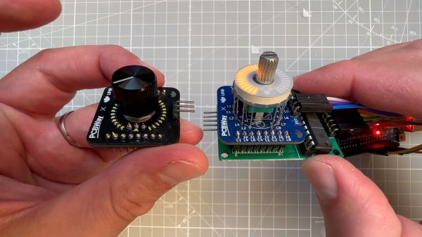
If there’s one thing we like around here more than seeing an improved version of a project we’ve already covered, it’s when the improvements make the original project cheaper. In the case of this LED ring light for pots and encoders, not only is it cheaper than its predecessors, it’s better looking and easier to integrate into your projects.

Right from its start, [upir]’s “Pimp My Pot” project has been all about bringing some zazzle to rotary controls. Knobs with a pointer and a scale on the panel are okay — especially when they go to eleven — but more lights mean more fun. The fun comes at a price, though; the previous version of “PMP” used an off-the-shelf LED ring light with a unit cost of about $10. Not the end of the world, perhaps, but prohibitive, and besides, where’s the fun in just buying a component specifically made for rotary control indication?

The new version shown in the video below is pin-compatible with the driver board [upir] used for the previous version, which is based on the MAX7219 display driver. Modifying the previous board to accommodate 32 white 0402 LEDs over a 270° arc was no mean feat. [upir] covers both creating the schematic and the PCB layout in some detail, providing his usual trove of tool-chain tips for minimizing the amount of manual work needed.

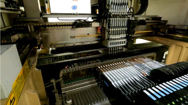
Wisely, [upir] chose to get his boards assembled by the vendor; getting all those LEDs to line up perfectly is a job best left to the robots. While the board is designed for use with pots that mount on either side, we much prefer mounting the pot’s shaft through the board, as it keeps the LEDs closer to the knob. The final price per board works out to about $6.30 in quantities of ten and falls to a trivial $1.70 each for lots of 1,000. Pretty sweet savings on a pretty sweet-looking build.

This is a cool use of a ring of LEDs, but if you prefer the finger kind, you can make that, too. You can do it the easy way or the hard way.

Continue reading “Pimp My Pot Redux, Now Cheaper And Even Better”

Tour A PCB Assembly Line From Your Armchair

Those of us who build our own electronics should have some idea of the process used to assemble modern surface-mount printed circuit boards. Whether we hand-solder, apply paste with a syringe, use a hotplate, or go the whole hog with stencil and oven, the process of putting components on boards and soldering them is fairly straightforward. It’s the same in an industrial setting, though perhaps fewer of us will have seen an industrial pick-and-place line in action. [Martina] looks at just such a line for us, giving a very accessible introduction to the machines and how they are used. Have a look, in the video below the break.

It’s particularly interesting as someone used to the home-made versions of these machines, to see the optical self-alignment and the multiple pick-and-place tools which are beyond the simpler pick-and-place machines you’ll find in a hackerspace. Multiple machines in a line are also beyond hackerspaces, so the revelation that the first machine is deliberately run slowly to avoid the line backing up is a valuable one.

At the end of the line is the reflow oven itself, through which the boards pass on a belt through carefully graded hot air zones. Certainly a step up from a toaster oven with an Arduino controller!

Sadly not all of us will be lucky enough to have such a line at our disposal, but pick-and-place projects come up here quite often. We did a teardown on the feeders from a Siemens machine a couple of years ago.

Continue reading “Tour A PCB Assembly Line From Your Armchair”

This Debug Connector Brings Your Issues To The Edge

Given an unknown PCBA with an ARM processor, odds are good that it will have either the standard 10 pin 0.05″ or 20 pin 0.1″ debug connector. This uncommon commonality is a boon for an exploring hacker, but when designing a board such headers require board space in the design and more components to be installed to plug in. The literally-named Debug Edge standard is a new libre attempt to remedy this inconvenience.

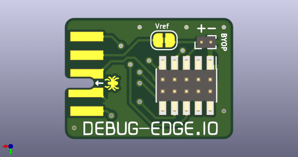
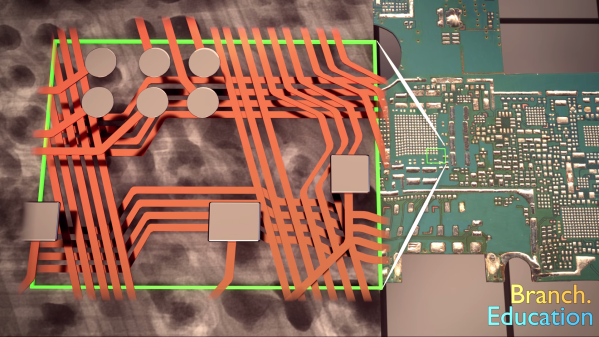
The name “Debug Edge” says it all. It’s a debug, edge connector. A connector for the edge of a PCBA to break out debug signals. Card edge connectors are nothing new but they typically either slot one PCBA perpendicularly into another (as in a PCI card) or hold them in parallel (as in a mini PCIe card or an m.2 SSD). The DebugEdge connector is more like a PCBA butt splice.

It makes use of a specific family of AVX open ended card edge connectors designed to splice together long rectangular PCBAs used for lighting end to end. These are available in single quantities starting as low as $0.85 (part number for the design shown here is 009159010061916). The vision of the DebugEdge standard is that this connector is exposed along the edge of the target device, then “spliced” into the debug connector for target power and debug.

Right now the DebugEdge exists primarily as a standard, a set of KiCAD footprints, and prototype adapter boards on OSHPark (debugger side, target side). A device making use of it would integrate the target side and the developer would use the debugger side to connect. The standard specifies 4, 6, 8, and 10 pin varieties (mapping to sizes of available connector, the ‘010’ in the number above specifies pincount) offering increasing levels of connectivity up to a complete 1:1 mapping of the standard 10 pin ARM connector. Keep in mind the connectors are double sided, so the 4 pin version is a miniscule 4mm x 4.5mm! We’re excited to see that worm its way into a tiny project or two.

We’ve seen plenty of part-free debug and programming connectors before. Have a favorite? Let us know in the comments!

Journey Through The Inner Workings Of A PCB

Most electronics we deal with day to day are comprised of circuit boards. No surprise there, right? But how do they work? This might seem like a simple question but we’ve all been in the place where those weird green or black sheets are little slices of magic. [Teddy Tablante] at Branch Eduction put together a lovingly crafted walkthrough flythrough video of how PCB(A)s work that’s definitely worth your time.

[Teddy]’s video focuses on unraveling the mysteries of the PCBA by peeling back the layers of a smartphone. Starting from the full assembly he separates components from circuit board and descends from there, highlighting the manufacturing methods and purpose behind what you see.

What really stands out here is the animation; at each step [Teddy] has modeled the relevant components and rendered them on the PCBA in 3D. Instead of relying solely on hard to understand blurry X-ray images and 2D scans of PCBAs he illustrates their relationships in space, an especially important element in understanding what’s going on underneath the solder mask. Even if you think you know it all we bet there’s a pearl of knowledge to discover; this writer learned that VIA is an acronym!

If you don’t like clicking links you can find the video embedded after the break. Credit to friend of the Hackaday [Mike Harrison] for acting as the best recommendation algorithm and finding this gem.

Continue reading “Journey Through The Inner Workings Of A PCB”

Analog Failures On RF Product Cause Production Surprise

A factory is a machine. It takes a fixed set of inputs – circuit boards, plastic enclosures, optimism – and produces a fixed set of outputs in the form of assembled products. Sometimes it is comprised of real machines (see any recent video of a Tesla assembly line) but more often it’s a mixture of mechanical machines and meaty humans working together. Regardless of the exact balance the factory machine is conceived of by a production engineer and goes through the same design, iteration, polish cycle that the rest of the product does (in this sense product development is somewhat fractal). Last year [Michael Ossmann] had a surprise production problem which is both a chilling tale of a nasty hardware bug and a great reminder of how fragile manufacturing can be. It’s a natural fit for this year’s theme of going to production.

Surprise VCC glitching causing CPU reset

The saga begins with [Michael] receiving an urgent message from the factory that an existing product which had been in production for years was failing at such a high rate that they had stopped the production line. There are few worse notes to get from a factory! The issue was apparently “failure to program” and Great Scott Gadgets immediately requested samples from their manufacturer to debug. What follows is a carefully described and very educational debug session from hell, involving reverse engineering ROMs, probing errant voltage rails, and large sample sizes. [Michael] doesn’t give us a sense for how long it took to isolate but given how minute the root cause was we’d bet that it was a long, long time.

The post stands alone as an exemplar for debugging nasty hardware glitches, but we’d like to call attention to the second root cause buried near the end of the post. What stopped the manufacturer wasn’t the hardware problem so much as a process issue which had been exposed. It turned out the bug had always been reproducible in about 3% of units but the factory had never mentioned it. Why? We’d suspect that [Michael]’s guess is correct. The operators who happened to perform the failing step had discovered a workaround years ago and transparently smoothed the failure over. Then there was a staff change and the new operator started flagging the failure instead of fixing it. Arguably this is what should have been happening the entire time, but in this one tiny corner of the process the manufacturing process had been slightly deviated from. For a little more color check out episode #440.2 of the Amp Hour to hear [Chris Gammell] talk about it with [Michael]. It’s a good reminder that a product is only as reliable as the process that builds it, and that process isn’t always as reliable as it seems.