Chip decapping videos are a staple of the hacking world, and few things compare to the beauty of a silicon die stripped of its protective epoxy and photographed through a good microscope. But the process of actually opening that black resin treasure chest seems elusive, requiring as it does a witch’s brew of solvents and acids.
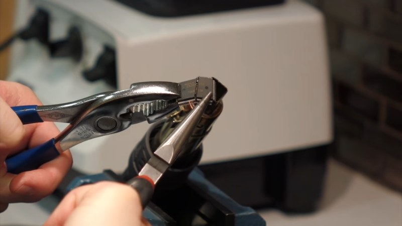
Or does it? As [Curious Marc] documents in the video below, a little heat and some finesse are all it takes, at least for some chips. The method is demonstrated by [Antoine Bercovici], a paleobotanist who sidelines as a collector of old chips. After removing chips from a PCB — he harvested these chips from an old PlayStation — he uses hot air to soften the epoxy, and then flexes the chip with a couple of pairs of pliers. It’s a bit brutal, but in most of the Sony chips he tried for the video, the epoxy broke cleanly over the die and formed a cleavage plane that allowed the die to be slipped out cleanly. The process is not unlike revealing fossils in sedimentary rocks, a process that he’s familiar with from his day job.
He does warn that certain manufacturers, like Motorola and National, use resins that tend to stick to the die more. It’s also clear that a hairdryer doesn’t deliver enough heat; when they switched to a hot air rework station, the success rate went way up.
The simplicity of this method should open the decapping hobby up to more people. Whether you just want to take pretty pictures or if reverse engineering is on your mind, put the white fuming nitric acid down and grab the heat gun instead.
Thanks to [killergeek] for the tip.


Has anyone tried this on blob chips?
Good idea. Let’s try. I have a few dead devices with blob chips.
I’ve managed to get some off by flexing the PCB. Basically left me with a die and bondwires still encapsulated in the blob itself.
I find it dangerous.
Not for the user mind you, people choose what they do and to protect themselve or not.
But for the chips.
I mean, if anyone can break up a chip, I hope that it never gets viral to youtube / instagram / TicToc / whatever.
Just imagine total newbee breaking an old chip, just to make some views.
“You will never find what append when I crack open an old ceramic 4004”
“I break a $2000 chip live!”
“How many chip can I broke in 1h? Let’s find out!”
“Wonder what’s inside a gameboy CPU? This video will interest you.”
Yeah, I’m old, I know.
But I think breaking a chip should be to create high definition shoot of it for retro engineering / archiving not just for fun.
Breaking a still in production chip is fine, but I bet that if it become easier, it can be used for profit by tech illiterate just willing to “make views” or be perceived “smart”.
The video itself is a great tutorial and will probably help decapers, I’m just grumpy I guess.
Do you want my box of misc old chips?
Realistically, old chips from failed boards are almost certainly going to get skipped instead.
I’m sorry, I don’t have the knowledge to properly decap it for an useful purpose.
Old chip from failed boards are the chip to decap ; If you can’t repair it, at least, document it.
Some people like Furrtek or other do that, and you can now have (some) VHDL description of old chips.
Contact them to give them you chip maybe?
I don’t think the clickbait youtubers will get the views they want from breaking chips.
Yeah, more likely they would just make another, “Refine gold from old computer chips” video.
Sadly, most of the profit is “watch me smash up a brand-new Iphone with a hammer”, or some acid, or a blowtorch or whatever. It turns out we live in a world where it’s financially viable to spend thousands of quid on top-end consumer goods, and destroy them with hammers, in return for the advertising money.
That corona virus can’t come fast enough.
Now that the virus is here, could you please ask it to go away ?
Thanks ;-)
Yeah, kids today and their smashing of technology for fun and profit, where the hell would they have got such ideas…
https://www.atlasobscura.com/articles/staged-train-wrecks
What you are saying is right.I remember when I watched a video in which someone destroyed a first generation IPhone.I was just so sad to see that people had no respect for old and rare technologies.Now, if the same thing happens with extremely difficult to find chips, some parts of our history might disappear forever.I just hope that nobody will be stupid enough to to do this kind of things.
Oooh… I used to do and teach failure analysis for “a big semiconductor” company and if your goal is just to get the die out to view, this might be OK. But as Dark Tiger says, this is probably hazardous to the chip’s health. The flex on the die would be bad and the pull of the leadframe off the substrate is probably not good either. Of course, if you know the chip is defective or you never intend to power it up again, I guess it would be OK. Motorola epoxy is pretty tough.
We had a pretty traditional process.
1) Use a mill to create a cavity that got as close to the die as you dared. Depending on the package size, that distance varied and we didn’t want to hit the tops of the bond wires.
2) Put the chip on a copper bar sitting on a hot plate under a vent hood. These were DIP packages so the legs straddle the copper bar. Wait about 1 minute.
3) Fill the cavity with fuming nitric. The vent hood is very important here as that stuff is nasty if it gets in your lungs.
4) Wait for it to stop bubbling (not long). Rinse with DI water and then alcohol.
5) Repeat until you see the die clearly exposed.
This will result in a chip you can still power up if you want to do testing. Bonus points. Without heat, you can put hydroflouric acid in the cavity and wait about a minute. Then rinse with DI/alcohol. Note that this is also NASTY stuff so if you don’t know how to handle very dangerous acid, figure that out first. Now you can take a microscope and look at one of the pad cuts. If you can focus on the top of the glass and the bottom of the pad, you need more acid (try about 30 seconds after the first minute). Eventually, you’ll find you can’t find the edge with the microscope focus and that means you will have removed the glass passivation.
My experience is maybe 50% – 60% will still work the same without the passivation, at least for a little while. But the success rate removing just the epoxy is very high if you have a little practice.
Now if you really want to do that, ask me how to sharpen a needle so you can probe and cut conductors.
Does it involve using the meniscus at the surface of concentrated sodium hydroxide to make a point only an atom across???
Sort of. We’d mount a piece of steel or tungsten wire in a holder attached to one side of an isolation transformer. The other side was an electrode in a beaker of NaOH. You repeatedly dip the wire. The tip gets attacked for the most time since it is the first in the solution and the last out. Halfway up gets less because it enters later and leaves sooner. Than the very back part just barely gets in and then it is out again. So that gives you the pointy profile. Don’t think it gets down to a single atom but you can get pretty small.
Like this: https://europepmc.org/backend/ptpmcrender.fcgi?accid=PMC2555190&blobtype=pdf
Cool, yah, in and out for the shallower angle… the single atom trick is how they do it for STM probes, letting the meniscus slide down the last bit of the tip until it cuts itself off, current has to be monitored I think. Think they’re using nichrome wire though. It’s been a few years since I was fully conversant with the whole procedure.
We used an ion beam to cut or add conductors.
You are younger than me ;-) We were just getting lasers to do cuts and they could even cut poly, but that was about the time I was leaving and we didn’t really trust them.
The fun thing about the needles was that you had to very barely touch them to the surface (they were mounted on lens positioners). But if you got impatient and drove the stage up into them (or forced them too hard down) you got a “Genie foot” where the needle curled up like the toe of a genie (djini) shoe.
That was a great video. It’s amazing I never though about just using heat to soften the epoxy.
I didn’t have any heat gun handy at the time I watch the video so I just tried the fan forced oven cranked up to max (260°C), using the tray I keep for solder reflow and all doors and windows open to get rid of the fumes.
I had to crack the packages a bit, put the chips back in a few minutes and so on. And I got some pretty good results.
As mentioned in the video, some dies are adhering to the epoxy rather then the lead frame (one out of four IC’s I decided to try this on)
I used that to have a peak inside a few IC’s I got from surplus merchants, some of which don’t have available datasheets.
Here are some photos taken a couple of hours after the video came out:
https://ibb.co/album/h8eNmF
Note that I’m only opening chips that either have no historical value or dead chips. It would be a waste to do that to a good SID chip or a working 6502.
I’m hoping to try probing some IC’s to see if they survive the treatment (260°C is actually pretty cold for a silicon die, if it doesn’t cool down too fast and crack). To could prove to be a great technique for reverse engineering chips.
Also, I’m pretty sure I once found a repository of sort, of silicon dies photos put together by a crowed that was reverse engineering IC’s. I would be happy to contribute with some photos if I can find the web page again.
Years ago I used to repair a lot of Alpha Micro computer boards. They used a lot of PLDs on their stuff and would blow the security fuse. I was able to decap them and figure out the fuse mapping and create replacement parts. They also used a PAL20X10 for a SSD software security device I was able to duplicate. It was a fun and useful endeavor. Of course this only worked on the ones with the fused link.
That’s an amazing story. How did you reconnect the fused link?
I didn’t reconnect the link. I used a microscope and copied the entire pattern of intact & blown fuses. Then I used some sacrificial devices to determine how the fuses were physically laid out on the device versus the pattern for the programmer.
I once decaped an IC by filing the epoxy on top until I got to the chip. If one does it carefully the chip won’t be damaged. Only the wires from chip to pin got filed out with the one I tried.
At work we somewhat regularly decap our own chips. If we just want to see where the damage is, we (well, I) mill off the top until I get beeps from a continuity meter hooked to the pins of the chip, meaning I’ve hit the bond wires, and then my coworker zippo decaps them: turns his zippo lighter sideways and waves the flame across the remaining epoxy. Usually it’ll just blow off after that kind of treatment, leaving the die exposed. Sometimes I have to flick bits off with an xacto blade under a microscope, because they cling on around the wire bond pads. This works with National Semiconductor parts. It’s pretty fast, and if you have a sacrificial identical chip, you can take pretty big cuts with the mill to figure out the right depth, and then put in the chip you care about and take off the whole layer in one big sweep and save a lot of time. (Use a two flute HSS milling bit.) Sometimes when you’re about 0.2mm above the top of the silicon the mill will start peeling the epoxy off the face of the silicon without even needing the zippo. When you mill this close you often touch the silicon along one edge because it’s hard to get the silicon precisely parallel to the mill table.
I’ve had surprising success on plastic and epoxy packaging with the following method:
1) Heat up whole package to orange hot with a propane torch
2) Allow to cool until it stops glowing
3) Heat up whole package to orange hot again
4) Tap away with a hammer and pinch with pliers to break of epoxy
It works 80% of the time, 20% of the time you break the die into still useful, but smaller fragments. It really is something to hold a bare die with tweezers and heat it up wit ha torch, as the glow is perfectly uniform on both sides.
Be careful, some chips contain Berillium, which is very toxic.!
Just tried this method, it works incredibly well!
I was using the torch method before. It’s really a pain in the ass to do and have many disadvantages:
– the biggest problems are the odors (really bad) and the toxic smoke
– it requires some time to do
– it can visually “damage” the die. You can see small cracks if the die has been burnt to orange and the traces are no longer in an uniform color. Result can be really good but is generally far from perfect.
With the Antoine method, I got multiple DIE extremely clean, without any visual damage, and it’s really quick to do (took me ~3min / chip). No more toxic smoke and bad odors, no more “damaged” die…
Btw there is a risk (but there are also some with the torch) if you don’t know the size/position of the die, you can crack it if you break the chip at the wrong place. This happened to me once on an IC with the die that was much bigger than usual.