Tuning a desktop router and your board designs for isolation routing can be a bit tricky, with thin traces usually being the first victim. For simple prototype boards you usually don’t need tightly packed traces, you just want to isolate the nets. To do this with a minimum amount of routing, [Michael Schembri] created kicad-laser-min, a command-line utility that takes a Kicad PCB design and expands all the tracks and pads to their maximum possible width.
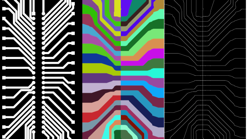
The software takes one layer of the PCB layout, converts it to black and white, and then runs a C++ Voronoi algorithm on it to dilate each track and pad until it meets another expanding region. Each region is colourised, and OpenCV edge detection is used to produce the contours that need to be milled or etched. A contour following algorithm is then used to create the G-code. The header image shows the output of each step.
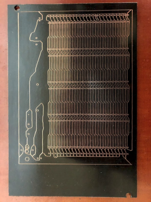
Full source code is available on GitHub. [Michael] has had good results with his own boards, which are scribed using a laser cutter before etching, but welcomes testing and feedback from other users. He has found that OpenCV doesn’t always completely close all the contours, but the gaps are usually smaller than the engraving width of his laser, so no shorts are created.
This is basically “Scribble style” prototyping with CAD and CNC tools. If you prefer scribe and etch, you might consider building a simple PCB shaker for faster etching. If you have a router but want to avoid the dust, you can use a carbide scribe to scratch out the tracks without needing to etch.


WOW, this is actually so useful!
How is this different to what pcb2gcode (https://github.com/pcb2gcode/pcb2gcode) does when passed the –voronoi option?
Should we ban all mentions of useful tools that are not unique?
Indeed, this tool is a nice example of wheel reinvention. Here’s another one: https://github.com/Traumflug/Visolate, based on an even older version developed at MIT in 2005: https://groups.csail.mit.edu/drl/wiki/index.php?title=Visolate:_Voronoi_Toolpaths_for_PCB_Mechanical_Etch
yeah visolate WOULD or COULD be quite usefull if it just be able to read gerber X2 files.
With ucamco, guess the inventor of gerber, gerberviewer i found out that the example is x1 and kicad just can create x2 types. So there is absolutely no use for this as x2 types garble only the screen.
I wish i had the knowledge or support to update it or even import into kicad as a module. men would i be glad.
A bit convoluted, perhaps? Why not print the Voronoi diagram and fix it up with Wite-Out and a Sharpie before scanning it and sending it to OpenCV?
How can you possibly think that is *less* convoluted than having it be completely automatic?
Whoosh!
>converts it to black and white
sure sounds good
>and then runs a C++ Voronoi algorithm on it to dilate each track and pad until it meets another expanding region
yeah still sounding good
>Each region is colourised
okay…
> and OpenCV edge detection is used to produce the contours that need to be milled or etched.
say what?!
That cannot be the best way to carry out this process… Doesn’t kicad have a built in pour functionality? It seems like a script to put a pour on each net would have been way easier and not involve running computer vision on your board layout
Kicad does not do voronoi pours. The first pour it processes will fill as much space as possible and restrict the size of the neighbouring ones.
OpenCV is just a set of image processing algorithms, it’s not some giant machine that’s overkill for trivial tasks. Using a contour tracing function from it is no different from using one from any other source or writing your own, except that it’s probably better.
But if you’re using a Voronoi algorithm don’t you already generally know where the edges are anyway? It just seems like an extra step.
You might want to look up how Voronoi is implemented; generally it’s done with only images as input and output. You *don’t* know where the edges are until you do an edge-finding step.
Gotta be honest, buying a desktop PCB mill that I’m currently trying to sell was one of my bigger regrettable purchases. If you really, truly, for real only need exactly one, there’s probably some expensive off the shelf solution that’s going to involve a lot less hassle, and might even be cheaper overall when you factor in shipping costs for parts, time, broken end mills, etc.
If this is purely a DIY excercise for the fun of it, there’s always etching. If you work for a big company that does this stuff, you can probably afford quick turn fab, or a really high end conductive ink printer or something.
For everything else, there’s OSHPark! Subtractive manufacturing was kind of shocking coming from 3D printing, I was surprised at how relatively unfun it is.
I highly doubt anyone with the determination and understanding of the capabilities you need to properly do CNC work is going to be discouraged.
There’s quite a few people who no longer bother with DIY PCBs anymore because of of cheap fab houses and the fact that one-hour PCBs aren’t really a priority for a lot of people.
I’d be really, really impressed if you can make PCBs with the quality and complexity of a commercial fab in an hour. Going with the pros lets you design *exactly* what you want and not be limited by the usual DIY via techniques.
Maybe it’s a different story if you regularly work on a lot of more experimental analog/RF/discrete silicon/through hole stuff, or if you’ve got ultra-steady hands and can do micro vias quickly, or you doing enough of this to justify a via plating setup.
But otherwise, I mostly hear people with typical cheap mills using 12+ mil traces, 0.8mm or larger vias, and if you want solder mask that’s a whole different process, so most people just skip it.
I’m not sure the typical hobbyist or even pro is going to be well served by dealing with all the limitations, unless very fast turnaround is a major priority, in which case yeah mills seem awesome.
But I’d rather wait a week and have a professionally made board with modern SMD parts, especially if it’s a personal project, and I probably won’t have time to write the code in less than a week anyway.
Sub-hour PCBs are a boon when you have part of a weekend to yourself, and some fairly straightforward design isn’t worth paying for fast shipping, or getting 3,much less several dozen of them (in the latter case, when if I have to pay more for shipping a design than the design itself, I’m going to want to maximize my yield).
What is a “modern SMD part” – the packages? BGA and fine pitch QFN and all those fun parts I wouldn’t want to solder at home, so am not about to design with? if I need a stencil, of course I’m going to send it out (I have a CO2 laser, but that can’t cut metal). I don’t have a reflow oven, but have no trouble home etching and hand soldering parts with 0.65 pitch (I just don’t intend to assembly line mode with them).
IMO, SMD makes home etching a preferable route for hobby work, because you don’t have to drill a ton of holes. If you can lay out your design for single-sided routing, or with just a couple of 0R to bridge signals, or route a wire or two across the backside of a PCB, home etch/route is a great way to have your design today and without too much fuss. Etching is nominal cost – less than US$20 to get started, milling isn’t that much more these days (US$200 at the low end for a 3018 mill). Even if your intent is to make a bunch of something eventually via a fab, it is a quick way to get to proof of concept for a circuit and components, even if the layout isn’t the same as final rather than sending a design out, getting a board back a week later for a premium, and THEN realizing you flubbed something (esp if you were in a rush to submit the design so you could get it back quick).
I honestly don’t see Voroni PBs as something anyone doing PCBs professionally would be looking to do, nor on ultra fine pitch footprints, but it would definitely cut down on etch or milling time in many designs.
If the PCB design is not HF/RF and the schematic is not verified or simulated in spice, which is just a mayor but not the final truth for stable operation especially for analog circuits. THEN a PCB converted into voronoi and milled that significant less traces length compared to plain EDA => isomilling is a good alternative.
Why order 5, 10, … prototype pcbs, waiting weeks to arrive, ….
spray painting the proto after soldering is fine for me if that 1 – 5 PCBs is all i need. If going into manufacturing 10 – …. PCBs it is worth to calc ALL from needed time, material (PCB & Parts, screws,….), quality, lcm including wastemanagement.
Broken bits are usually a matter of stupidity to lack of experience for speed, rev, …. If someone ever has milled plastic or alloy, not only some mm, s/he knows about params like chipload, grease, cooling, mist, … for stable cutting.
Most if not all cheap mills need a little rework like my 3018 from asia. T8 axles fixation and reverse gap was shitload. I made M6 on a lathe on all ends and fixed with usual M6 nuts instead of weak self losening M2 screws. Reverse gaps significantly reduced by pre-springloading the nut.
mill motor the fanblade was imbalanced which made horrible noise & wobbles the whole machine not to mention the bearing stress. plain balancing on a glas plate improved wellllll but when a new fanblade arrived it was history at all.