JavaScript App Uses Advanced Math To Make PCBs Easier To Etch

We all remember the litany from various math classes we’ve taken, where frustration at a failure to understand a difficult concept bubbles over into the classic, “When am I ever going to need to know this in real life?” But as we all know, even the most esoteric mathematical concepts have applications in the real world, and failure to master them can come back to haunt you.

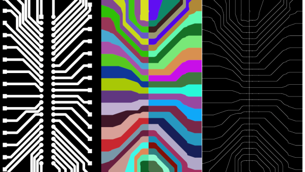
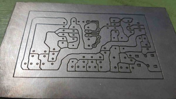
Take Voronoi diagrams, for example. While we don’t recall being exposed to these in any math class, it turns out that they can be quite useful in a seemingly unrelated area: converting PCB designs into easy-to-etch tessellated patterns. Voronoi diagrams are in effect a plane divided into different regions, or “cells”, each centered on a “seed” object. Each cell is the set of points that are closer to a particular seed than they are to any other seed. For PCBs the seeds can be represented by the traces; dividing the plane up into cells around those traces results in a tessellated pattern that’s easily etched.

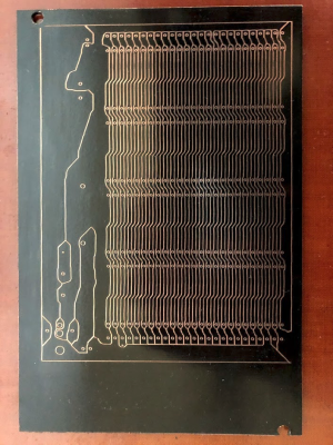
To make this useful to PCB creators, [Craig Iannello] came up with a JavaScript application that takes an image of a PCB, tessellates the traces, and spits out G-code suitable for a laser engraver. A blank PCB covered with a layer of spray paint, the tessellated pattern is engraved into the paint, and the board is etched and drilled in the usual fashion. [Craig]’s program makes allowances for adding specific features to the board, like odd-shaped pads or traces that need specific routing.

This isn’t the first time we’ve seen Voronoi diagrams employed for PCB design, but the method looks so easy that we’d love to give it a try. It even looks as though it might work for CNC milling of boards too.

Transform Kicad Design To Patchwork For Isolation Routing

Tuning a desktop router and your board designs for isolation routing can be a bit tricky, with thin traces usually being the first victim. For simple prototype boards you usually don’t need tightly packed traces, you just want to isolate the nets. To do this with a minimum amount of routing, [Michael Schembri] created kicad-laser-min, a command-line utility that takes a Kicad PCB design and expands all the tracks and pads to their maximum possible width.

Laser scribed PCB with maximum track widths

The software takes one layer of the PCB layout, converts it to black and white, and then runs a C++ Voronoi algorithm on it to dilate each track and pad until it meets another expanding region. Each region is colourised, and OpenCV edge detection is used to produce the contours that need to be milled or etched. A contour following algorithm is then used to create the G-code. The header image shows the output of each step.

Full source code is available on GitHub. [Michael] has had good results with his own boards, which are scribed using a laser cutter before etching, but welcomes testing and feedback from other users. He has found that OpenCV doesn’t always completely close all the contours, but the gaps are usually smaller than the engraving width of his laser, so no shorts are created.

This is basically “Scribble style” prototyping with CAD and CNC tools. If you prefer scribe and etch, you might consider building a simple PCB shaker for faster etching. If you have a router but want to avoid the dust, you can use a carbide scribe to scratch out the tracks without needing to etch.

A Dual Screen Luggable With Integrated RTL-SDR

It’s been fascinating to watch the development of bespoke mobile computers go from a few sheets of foam board and a Raspberry Pi into hardware that looks like it’s actually been transported here from an alternate reality. Granted a Raspberry Pi is more often than not still onboard, but the overall design and construction techniques of these very personal computers has improved by leaps and bounds.

The latest of these cyberdecks, a dual screen “luggable” reminiscent of classic computers like the Compaq Portable or Kaypro, comes our way from [dapperrogue]. Powered by the Raspberry Pi 4 and featuring a scratch-built mechanical keyboard to perfectly fit the machines’s specific dimensions, this is easily one of the more practical builds we’ve seen. As visually striking as they may be, few would argue that the small offset display that seems characteristic of most decks are ideal from a usability standpoint.

While the keyboard plate was milled out on a CNC, [dapperrogue] says the design of the HDPE body panels and rear polycarbonate viewing window were simple enough they could be done by hand on a band saw. The PETG internal frame uses a Voronoi pattern that not only reduces the amount of time and material required to print it, but maximizes airflow. The fact that it looks like some kind of alien biological life form only helps the retro-futuristic aesthetics.

There’s still plenty of room inside the enclosure, which is good, as [dapperrogue] says there’s more goodies to come. Adding internal battery power is a logical next step, and now that the Pi 4 can boot to external drives, and SSD is also on the list of future upgrades.

For readers who might be getting a sense of déjà vu from this project, [dapperrogue] notes this design was inspired by the phenomenal Reviiser that [Dave Estes] released earlier this year.

Making A Gorgeously-Twisty Sculpture, Using Only Flat Pieces

Closeup of unique pieces that make up the final scuplture.

The sculpture shown here is called Puzzle Cell Complex and was created by [Nervous System] as an art piece intended to be collaboratively constructed by conference attendees. The sculpture consists of sixty-nine unique flat panel pieces, each made from wood, which are then connected together without the need for tools by using plastic rivets. Everything fits into a suitcase and assembly documentation is a single page of simple instructions. The result is the wonderfully-curved gyroid pattern you see here.

The sculpture has numerous layers of design, not the least of which was determining how to make such an organically-curved shape using only flat panels. The five-foot assembled sculpture has a compelling shape, which results from the sixty-nine individual panels and how they fit together. These individual panel shapes have each been designed using a technique called variational surface cutting to minimize distortion, resulting in their meandering, puzzle-piece-like outlines. Each panel also has its own unique pattern of cutouts within itself, which makes the panels lighter and easier to bend without sacrificing strength. The short video embedded below shows the finished sculpture in all its glory.

Continue reading “Making A Gorgeously-Twisty Sculpture, Using Only Flat Pieces”

Copper Coil Lamp Built With 3D Printed Tools

3D printing is a great way to create complex geometric forms. However, it can be very slow, and parts may lack strength compared to other alternatives. There are other ways to take advantage of this technology however, as shown in the build of this tidy voronoi lamp. 

The lamp is so-called for its voronoi-patterned base, named after the mathematical concept. 3D printing is used to create the base, which would be very difficult to create with traditional subtractive machining methods. A copper coil is then used to give the lamp some height, as well as act as protection for the filament bulb. Here, 3D printing helps out in a different way, being used to create a jig to allow the copper to be quickly wound into an accurate coil shape. The coil also serves to act as a conduit for the mains wiring, giving the lamp a neat finished appearance.

The project goes to show that even if 3D printing is appropriate to produce your final parts, it may be of help to create useful jigs or tools to get the job done. We’ve even seen similar applications before in the microcontroller space!

The Trompe-l’œil Menorah

Hanukkah decorations have been up in stores since before Halloween, and that means it’s time for electronic Menorahs with blinking LEDs, controllers, and if you’re really good, a real-time clock with support for the Jewish calendar. [Windell] over at Evil Mad Scientist just outdid himself with the Mega Menorah 9000. It’s a flat PCB with nine LEDs, but it uses stippling and a trompe-l’œil effect to make it appear three-dimensional.

Making a 2D object look three-dimensional isn’t that hard – you just need the right shading. A few years ago, [Evil Mad Scientist] created StippleGen, a library to turn images into something that can be easily reproduced with the EggBot CNC plotter. It’s actually quite impressive; there are Voronoi diagrams and travelling salesmen problems, all to draw on eggs. The library can be used for much more, like properly shading a PCB so that it looks three-dimensional.

The Mega Menorah 9000 is surprisingly large, at about 7.5″ wide. It’s powered by an ATtiny85 loaded up with the Adafruit Trinket firmware, making it a truly USB enabled Menorah. While it may just be a soldering kit, it is a fantastic looking PCB, something we’d like to see some more examples of in the future.