With all the cool and useful parts you can whip up (relatively) quickly on a 3D printer, it’s a shame you can’t just print a PCB. Sure, ordering a PCB is quick, easy, and cheap, but being able to print one-offs would peg the needle on the instant gratification meter.
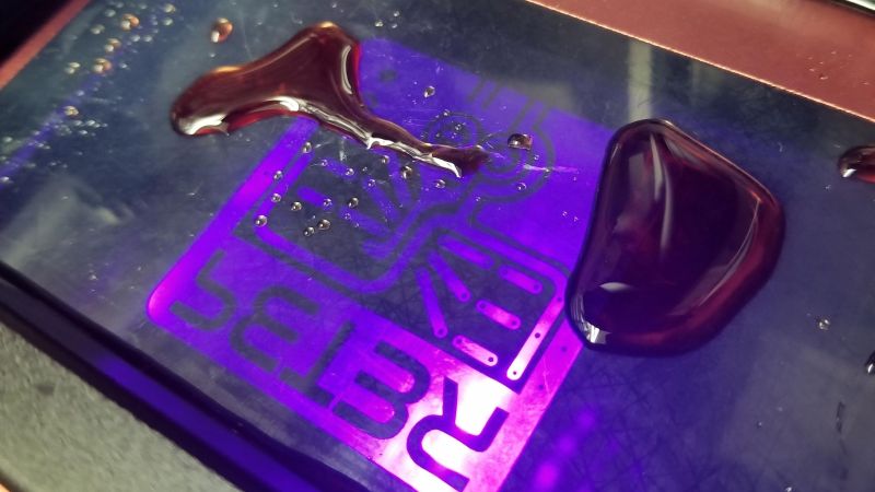
[Peter Liwyj] may just have come up with a method to do exactly that. His Instructables post goes into great detail about his method, which uses an Elegoo Mars resin printer and a couple of neat tricks. First, a properly cleaned board is placed copper-side down onto a blob of SLA resin sitting on the print bed. He tricks the printer into thinking the platform is all the way down for the first layer by interrupting the photosensor used to detect home. He lets the printer go through one layer of an STL file that contains his design, which polymerizes a thin layer of plastic onto the copper. The excess resin is wiped gently away and the board goes straight into a ferric chloride etching bath. The video below shows the whole process.
As simple as it sounds, it looks like it works really well. And [Peter] didn’t just stumble onto this method; he approached it systematically and found what works best. His tips incude using electrical tape as a spacer to lift the copper off the print surface slightly, cleaning the board with Scotchbrite rather than sandpaper, and not curing the resin after printing. His toolchain is a bit uncoventional — he used SketchUp to create the traces and exported the STL. But there are ways to convert Gerbers to STLs, so your favorite EDA package can probably fit in to the process too.
Don’t have a resin printer? Don’t worry — FDM printers can work too.
Thanks to [abetusk] for the tip.


wonder if you could put it back in an print a solder mask on it.
Working on it. I should have a masked board by this weekend!
Since you’re reading the comments, can you print a PCB test pattern that has a range of trace widths?
It’d be really awesome if the method could be used to make thin traces reliably.
“PCB test pattern” in google will find you several, if you don’t already have one.
I am guessing it can do 5mil all day.
After a bit of fine tuning I print/etch traces down to .2 mm, gaps at .5mm and holes with a 1mm diameter. Traces I use are .5 mm I see no need to make them smaller since I don’t use SMD stuff yet.
I already have a file up with line widths and gaps from 0.1 mm to 1.0 mm I will be trying it this weekend. Check at the bottom of this instructable. I will be trying it with different gaps and maybe exposure times. Running a bit low on boards but I’ll try a few.
Very cool. Keep us updated as to how well it works! I’ll check your youtube channel in a few days.
Now that is a great question.. I don’t see why not myself – though how good a solder mask any of the resins will make is the question there..
UV curing solder mask available from Asia in all the standard colors, they are normall screen printed. it will work here.
Only if the masks designed for screen printing are going to polymerise with the printers UV output, not harm the print tray, and cover the board in this setup.
A good point though, and it should work, experimentation required.
This is actually the only use I think I’d put a SLA printer to – that has to do with PCBs, other uses are plentiful.. I didn’t have any trouble what feels like eons ago with a laser printer – so why change methods unless it gets you something more, like easy solder masks.
Experimentation should be easy.
Most current printers use FEP stretched over either a metal or PLA frame/container. (Possibly other plastics.) Older ones used solar panel protectant and things like nagaline (sp?) or polycarbonate. (Acrylic doesn’t work with most and melts.) Test each and find out.
It makes an excellent solder mask. I used the tip of an exacto knife to put a bit of resin at the trace just at the edge of each pad then zapped it with a UV light. The solder did not leave the pad. I think I may paint the board with resin and set it off to act as a sort of mask and conformal coating.
Now someone only needs to find a clever way to reference the board, e.g. with some 3d printed frame, to the machine so you can do double sided boards.
That doesn’t seem hard as the tanks are very dimensionally accurate – so just make the blank boards fit to the edges/ have the printed spacer to put them where you want
I guess, people already used this for exposure of classic uv masked PCBs (did not google yet). Gets 50% of the hassle out of the game. ;)
And what a supprise… ;)
https://hackaday.com/2018/11/24/put-that-dlp-printer-to-use-making-pcbs/
Guess someone should have added “Its been done already…” to the HaD comment bingo…
https://hackaday.com/2020/10/08/hackaday-passes-1000000-comments/
that’s the “issue”, if one can not edit his own comments.
Just try to read it as one comment, if your sense of order got tickeled too much. ;P
Could you simplify this, get uv coated PCB, the screen and the blacklight and directly expose the design onto the PCB?
Like the “old” method, using a transparency and a UV light box, but with a screen as the transparency?
I am working on this very approach now except I am not interested in single sided boards, everything I do is double sided complete with riveted vias etc. I even add a pretty decent solder mask too.
My printer only arrived yesterday so a ways to go yet. My biggest challenge is making a centering device that will allow board flipping with excellent accuracy
And sorta
https://hackaday.com/2014/01/14/creating-pcbs-with-3d-resin-printers/
People also used Epson printers to put a mask on naked copper boards?
https://hackaday.com/2012/04/24/printing-pcbs-on-a-junked-epson-printer/
I recall a less modified printer being used as well. Nothing wrong with OP, using a tool for more than one purpose is good. But I wouldn’t go out and buy a resin printer to make PCBs. Too messy.
No if your going to buy a tool for pcbs first and other stuff second get a laser or mill
I bought the resin printer to do resin prints. Not for making PCBs. This is just an interesting side project.
What we really need is a way to just easily print traces without the chemical baths. That would be the cats meow for most projects. If the conductive material is somewhat flexible even better. Other thought was use the 3D printer to leave channels that you could fill with a conductive material…. Print, then paint, then wipe off the excess with a straight edge and you have a PCB…. Wishful thinking…. I suppose.
I have a black only laser printer that I intended for making my own pcbs…. but haven’t yet due to the intimidating chemical baths for etching process…. Still on my todo list to try though!
use the right chemical and you only need the one tank of it – Cupric Chloride if memory serves is the best choice. Use it, when it starts to fail bubble lots of air through it and it starts to work well again.
Does mean you have a tank full of the stuff kicking around all the time – but its pretty safe, effective stuff as I recall. And the bubbling bar from an aquarium or something to refresh it can also be used to agitate the surface at the PCB keeping fresh acid at the copper for even etching.
Various entities have tried to use printers (3D and inkjet) to put down conductive traces but I’ve yet to see one that really works w/o compromise. I’ve often mused whether an old technology couldn’t be brought back to life, if only for the hacker and average home enthusiast, given todays low cost machinery. That tech being MultiWire. We used that quite a bit back in the ’80s and it worked until density and speeds became too high. Things that most “home” PCBs don’t have to contend with.
One option I can see with the level of detail SLA printers are capable of is to make them the substrate of the board – all the traces are grooves in the faces, print the through holes too – then copper deposition coat the whole thing and sand off the excess copper leaving it only in the printed recess and via.
With the price of SLA resins not a particularly cheap method but you are really printing the desired circuit and can do 2 sided boards easily enough. Also have to ask what resin can really take the heat cycle abuse of soldering steps and isn’t too brittle for practical use (I’m not aware of any).
Can take the heat?
None.
Best you can get is a max around 250°C and that is probably only for very short cycle times.
You could print a mold, but then you’re getting into too many process steps.
I wouldn’t mind a process using copper tape and wood. Much easier on drill bits. Just throwing it out there…
Try painting your resin onto some plastic film that the resin does not bond with then lay the film onto the PCB so that the resin is between the two, if it works it will save a lot of clean up time and materials too, particularly if the film is reusable. Just peel it off and pop the pcb in the etching bath.
Assuming you are referring to the resin 3D printer method:
There is already a thin (non-stick) film called “FEP film” between the screen and the resin. It’s designed to just peel off and be reusable, because that’s how the printer works.
You can’t “paint” standard resin on because the surface tension will make it form droplets. To get a thin layer, like 0.05mm, you need to sandwich the resin between the screen and “print bed” (pcb).
I used a method similar to this to “mask” the pins on a particularly stubborn SMD chip prior to micro-soldering.
Ended up finding a nice resin pen at the car accessories shop but had to modify its attached LED as it sucked.
added an Al casing from a smashed flashlight and this works well as a heatsink and casing with a parallel resistor across the LED to guard against static damage and some nice long wires to plug it in to a constant current driver.
Now where can I purchase a refill? £17 is a fair chunk of change.