One of the exciting trends in hardware availability is the inexorable move of FPGA boards and modules towards affordability. What was once an eye-watering price is now merely an expensive one, and no doubt in years to come will become a commodity. There’s still an affordability gap at the bottom of the market though, so spotting sub-$20 Xilinx Zynq boards on AliExpress that combine a Linux-capable ARM core and an FPGA on the same silicon is definitely something of great interest. A hackerspace community friend of mine ordered one, and yesterday it arrived in the usual anonymous package from China.
There’s a Catch, But It’s Only A Small One
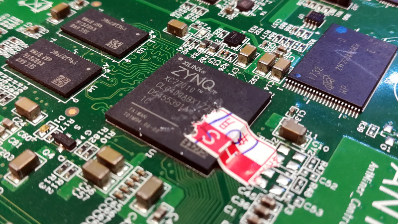
There are two boards to be found for sale, one featuring the Zynq 7000 and the other the 7010, which the Xilinx product selector tells us both have the same ARM Cortex A9 cores and Artix-7 FPGA tech on board. The 7000 includes a single core with 23k logic cells, and there’s a dual-core with 28k on the 7010. It was the latter that my friend had ordered.
So there’s the good news, but there has to be a catch, right? True, but it’s not an insurmountable one. These aren’t new products, instead they’re the controller boards for an older generation of AntMiner cryptocurrency mining rigs. The components have 2017 date codes, so they’ve spent the last three years hooked up to a brace of ASIC or GPU boards in a mining data centre somewhere. The ever-changing pace of cryptocurrency tech means that they’re now redundant, and we’re the lucky beneficiaries via the surplus market.
Getting To The Linux Shell Is This Easy!
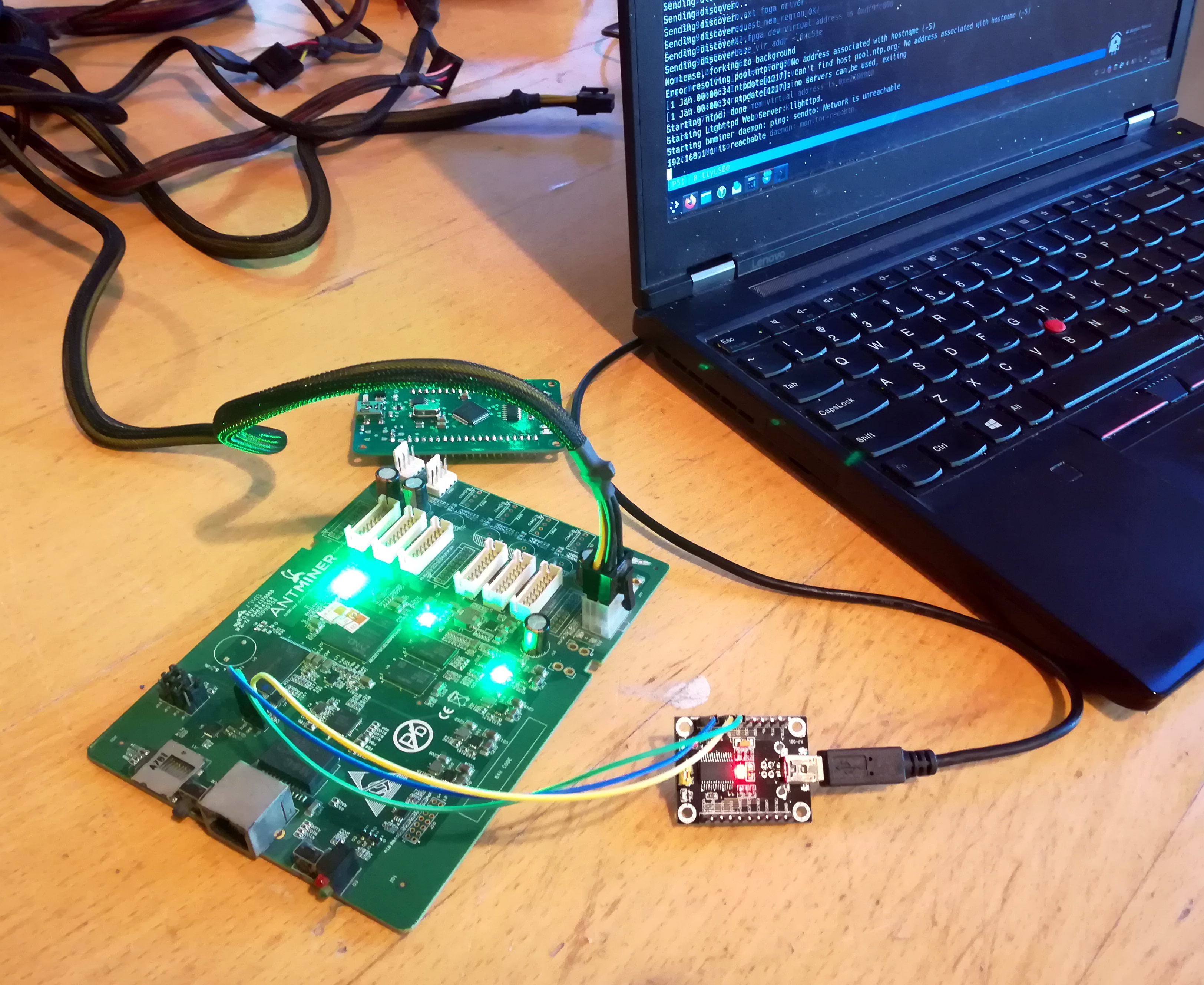
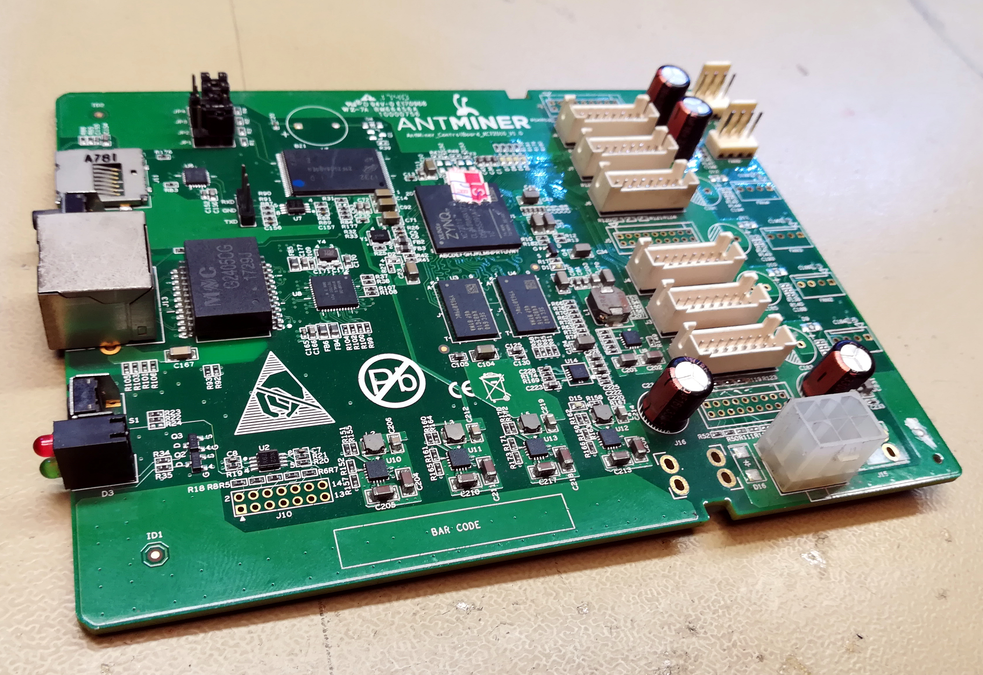
On the PCB is the Zynq chip in a hefty BGA with its I/O lines brought out to a row of sockets for the miner boards, Ethernet, an SD card slot, a few LEDs and buttons, and an ATX 12V power socket. The serial and JTAG ports are easily identifiable and readily accessible, and connecting a USB-to-serial adapter to the former brought us to a Linux login prompt. A little bootloader shell wizardry allowed the password to be reset, and there we were with a usable shell on the thing. Changing a jumper allows booting from the SD card, so it would be extremely straightforward to bring your own ARM Linux build onto the device to replace the AntMiner one, and since the Zynq can load its FPGA code from within Linux this makes for an extremely accessible FPGA dev board for the price.
These boards seem to be offered by multiple vendors, which indicates that there must be quite a few in the supply chain. Stocks will inevitably run out though so don’t despair if you fail to snag one. Instead they are indicative of a growing trend of application specific FPGA boards being reimagined as general purpose dev boards by our community (for example the Lattice FPGA in a hackable LED driver board we featured back in January). It’s a fair certainty that they’ll be joined by others as their generation of FPGA tech starts to be replaced.
We’ll be keeping our eye out for any others and we’re sure you’ll drop us a tip if you see any.


a word of warning on these antminer rigs, they have a tendency to “dew up” in humid environments and the end result is corrosion around the FPGA, i think rossman did a video on one (or it might have been eevblog 2 min tear down)
I’m a complete amateur here but would the be resolved by coating that section (the pins), with silicon gel or something similar?
But did the original owner do that?
I thinking [darkspr1te] is warning us that some may arrive already corroded.
Only if you try to cool them with an air conditioner as illustrated in that rossman video. Mining for years and haven’t seen a speck of rust.
s/7000/7007/g
There is no “Zynq 7000” part; instead 7000 is used to describe the entire family.
Ha! There’s not even a Zynq 7007. It’s actually a 7007s. (The ‘s’ suffix stands for “single” meaning one of the two ARM cores has been disabled by a fuse.) It’s the same die as the 7010. All 28k logic cells are there, but the software (not the chip) limits you to using only 23k of them at a time. The ‘7007s block RAM is limited to 5/6 of the ‘7010 capacity in the same way.
Couldnt you use one of these boards which actually stipulates the dual core version in the description ? £12.15 delivered to the UK doesnt seem too bad.
http://www.aliexpress.com/item/1005001500766274.html
As a novice to FPGA, what would you use the board for ?
That is a different board, I have such (EBAZ4205).
Find information what you can do with that board in this a month onld hackaday arcticle:
https://hackaday.com/2020/11/18/hacking-the-fpga-control-board-from-a-bitcoin-miner/
>As a novice to FPGA, what would you use the board for ?
You spend your free hours trying to get it to work in the first place. I don’t think there will be time for anything else.
A lot of jokes here but the best use of an FPGA is robotics or controlling other complex hardware. The other use is processing that is simple but needs to be done faster then the CPU can do. typically this is signal processing like video decoding or encrypting a high speed interface.
Use the FPGA any place you wish you have specialized hardware.
What can you do with it?
cofee
while rickrolling
replace a 555
and a few arduinos
all at the same time
Forgot the most important: blink an LED :P
That is a lot like asking what can you do with a paint brush.
Depending on the task you can easily get a good few gigaFLOPS of performance out of it.
(e.g. https://www.eetimes.com/how-to-build-ultra-fast-floating-point-ffts-in-fpgas/ )
The XC7Z007S has two 12-bit 1 MSPS ADCs with up to 17 Differential Inputs so you could make a SDR out of it.
It is like staring at a blank sheet of paper, what you can do with it depends on you.
Can I make a file server with a blank sheet of paper? Will the sheet run linux? Can I make a DNS ad blocker?
Yes, hold the piece of paper between you and the ads displayed on your monitor in a way that it blocks you from seeing the ads!
With this sheet… sure. It’s un-lined paper, so it might be harder than dealing with a RasPi though…
There are probably IP blocks for SATA, USB, etc, but I don’t know how far 28k is going to go… but with a 12-bit 1 MSPS ADC with differential inputs, I suppose you could even try to rig up an analog MFM RAID setup…
Yes, but will it run Crisis?
Whatever you do with it will require using Xilinx tools, which is enough for me to leave these boards for the recyclers when Lattice options are available now.
Yosys can already synthesize for Xilinx Series 7 and people are working on nextpnr to do place and route for these chips.
Dupe!!!
https://hackaday.com/2020/11/18/hacking-the-fpga-control-board-from-a-bitcoin-miner/
That is a different surplus cryptominer control board so not 100% a dupe…
This is good news. More the merrier.
Except this new one has *no* technical info other than the aliexpress link. It talks about the JTAG, serial connections, but *not* how. There aren’t any links on reverse engineering. So this is a weak one compared to the original.
The schematics for this board are posted at the end of the previous article. I’ve got mine running ubuntu’s core raspi armhf build off the sdcard. Planning on using it for a home automation gateway
Thanks. Found it in the comment section, so save everyone a click:
https://github.com/KarolNi/S9miner_sample
I got offered 6 of the antminers by the apartment supervisor, but only took one out of curisority. :(
My comment for how weak this newer article is still holds.
Good point, but not quite. This is a different board, and it only serves to further underline what I said at the end of the piece, that we’re in an age of cheap second hand FPGA boards.
So once we learn how to adjust to the FPGA way of thinking about programming, we can use our mad skills to stay in the job market.
Looks like this is dupe because the version supposed to show up in linked search is all gone :)
I wonder if this is a good platform to get started on RISC-V on FPGA development.
Yes, as you can load the bitfile from the arm under linux, use part of DDR for your risc-v core while having access from the arm (requires some work). And ~20k lut allows you to have a good risc-v core (but probably not big 64bits ones, need to check).
That is cool, I’m definitively gonna have to order one.
This Bob just did, x2 for delivery late January. Thank you, Jenny List.
Any time!
I’m not Bob, and neither’s my wife. But i’m not going to leave FPGA boards there at that price. They can sit in the same cupboard as the Nexsys2s I bought 12 years ago…
My question is when is appropriate to use an FPGA vs a general purpose compute platform. The difference to me seems to be higher performance running on an FPGA at the cost of higher programming complexity. Seems similar to the old RISC vs CISC debate which was settled when CISC processor became fast enough for 99% of compute needs. Or am I completely wrong about the use cases?
The traditional rule for CPU vs FPGA is that a CPU can have software developed for it 10x faster, but you are limited to the sequential speed of the CPU at processing data and instructions. With a FPGA gateware you are literally designing circuits, so in a FPGA everything can happen at once and everything can all happen in parallel, multiple times (depending on the available resources). And that difference is how a slow (few hundred MHz) FPGA can win a race against a much faster CPU (GHz) or multiple CPU’s, while using much less power.
If you are using a FPGA as a general purpose compute platform, then you are disabling most of the advantages of a FPGA. The key advantage of a FPGA is flexibility, but the major disadvantage is the development time.
Disadvantages of the FPGA include low clock frequency, limited logic count (especially the affordable ones), and poor memory bandwidth, compared to a CPU.
Memory bandwidth – maybe. Memory latency? Unparalleled (as long as you do not touch external DDR).
I could never understand this argument. FPGAs are far easier to program than anything sequential. Where does this myth of complexity of FPGA development come from?
FPGAs are hardware not code, so you need to think differently
[citation needed]
If HDL programming is easier than procedural programming, why is “the next big thing” in the FPGA world supposed to be high-level synthesis (HLS), where you can write sequential C/C++ code and have it translated into hardware?
HLS existed for ages, never became a big thing and never will. It is a solution searching for a problem, and that problem does not exist yet.
HLS is a big win, but not an easy win. A company can reduce the size of their FPGA development team from say 5 down to 1, but they’ll need to add someone who can handle the complexity of HLS tools. It’s not enough to know C or C++ to write these languages for high-level synthesis. One must have deep architectural knowledge of the target device, the bandwidth of the target device, and enough understanding of what the HLS compiler can and cannot do.
FPGAs can get you multiple of orders of magnitude better performance per watt over the best CPUs, but only for suitable problems and only if the developers know what they’re doing. Very tantalizing!
The complexity of FPGA development is no myth. For large projects, there are many aspects to this. Getting the design to fit the device, achieving timing closure, working around bugs in 3rd party IP, working around vendor toolchain issues, troubleshooting PCB designs. The list goes on and on. It’s all the stuff they don’t have time to get into in school. It can even come down to hardware errors in the FPGA itself, like signal integrity issues between the stuff that monitors the FPGA configuration for soft errors and some high-speed transceiver.
Many of these problems are not unique to FPGAs, but tend to be addressed upstream of typical application developers developing on established microprocessors.
I see FPGAs more often used for complex IO than for signal processing.
+1 and especially where there is hard real time, for example in mobile comms where timing constraints are very tight and we can’t put up with the vagaries of a CPU’s interrupt latency.
As someone who’s worked with CPU/GPU/FPGA professionally for a few years now here is the rule.
Does the task require many instances of the same operation to happen at the same time? Use a GPU. These are ideal because of how they manage computations in a sort of block fassion where data is provided an operation is selected and results are all calculated in parallel.
Does the task require performing many different tasks all at the same time? Use an FPGA. In an ideal world you would do as much as possible via this method. Think this way, if the CPU runs 10x faster then the FPGA but the FPGA is performing 100 jobs a cycle the FPGA is 10x faster in the end. In relaity FPGA development is very complex as making sure all these parallel things line up and don’t run over eachother is very difficult and certain computations simply don’t attribute themselves to parallel operations.
Else: CPU. CPU is the most general purpose solution and works when all else fails. It is by far the easiest to program but I feel this is mostly because it’s the oldest and so languages have become well flushed out. I think languages like VHDL are very good once you understand them but they are clunky at first and most lessons online do not help. Trying to learn FPGA programming by translating it to CPU equivalents is a BIG mistake. They are not the same and there is no equivalence, you are designing circuits so you must thing in terms of circuits. Trying to translate is kind of like learning a second language, the people I know who do it best express that they think in the second language they do not try and translate to the first.
One obvious use case: real time (when timing is nanoseconds tight). Also, anything that requires tons of pins
FPGA programming complexity is overrated. It is just different, but not more complex.
And it is not about performance primarily, it is about real time and predictability. Yes, you can bit bang, say, a VGA image out of an MCU. But it is hard. Bit banging on an FPGA is natural and easy.
What tool chain are people planning on using with these? Vivado licenses aren’t cheap and the ‘free’ version doesn’t generate configuration bitstreams for the FPGA last I checked.
Looks like your info is out of date to me – webpack supports Zynq 7000. See
https://www.xilinx.com/products/design-tools/vivado/vivado-webpack.html#architecture
I didn’t see bitstream generation on the page you linked.
Vivado handle all synthesis/placement/bitstream generation, so when a device is supported, everything is supported (even some hw IPs).
this is not true. 7010 is free
for anything but the biggest FPGAs the free webpack has always been fully functional
Would these have been overclocked (in other words, overheated) by the original owner(s)?
The FPGA isn’t mining anything, just controlling the miners. So probably not?
fpga are not like CPU, yes it is possible to overclock them, but in fact you are mostly limited by design speed (worst timing situation) so it’s mostly pointless.
You don’t exactly overclock a FPGA. There are trade offs between complexity vs speed. You set up the constraints on how fast you want you design and the place & fit would *try* to meet the timing needed assuming that there is sufficient on-chip resources it can use and the constraint isn’t out of whack with reality.
As for thermals, the FPGA is only used to control the data flow of the mining and nlt the actual computation. There isn’t much going on judging from the amount of I/O going to each mining card – just I2C and a single ended Tx/Rx. i.e. they don’t even need high speed differential pais.
I’ve been running a class on top of Artix7 dev boards for a couple years so I have a WebPack-licensed Vivado install on the machine I’m sitting at. I just re-targed a project to generate for a xc7z010clg400-1 (which I _think_ is what I read off the seller picture on the one I just impulse bought off Aliexpress) and it looks like it’s fully supported.
…Not sure why that didn’t show up as a reply to the folks discussing if it had WebPack support.
Continuing my reading, there is https://github.com/xjtuecho/EBAZ4205 that has some substantial RE documentation on probably the same board, and https://github.com/blkf2016/ebaz4205 looks like they have an XDC constraint file that matches the pinout, so these should be straightforward to get going.
But if you don’t have a schematic or a fpga example project … How can you really make something with fpga logic to interface the fpga with peripherals?.
I don’t see this..
I looks like it has already been reverse engineered, documentation and schematics here https://github.com/xjtuecho/EBAZ4205 and someone has written a constraint file (XDC for Vivadio) here https://github.com/blkf2016/ebaz4205
Should work the same as any other Zynq dev board with that information.
FYI: https://www.aliexpress.com/item/1005001793006194.html
Z4205 breakout board with VGA and camera connector – some soldering required for those through hole connectors. There seems to be additional info in the manual.
The best part is that this is Xilinx, which is now AMD, who are starting to release open source support for FPGA cores. Cross your fingers, and maybe you’ll see an open toolchain before long for it.
Had quite a few wondering why a GPU/CPU company would be buying an FPGA company. Doesn’t really fit into anything they do, and most likely not help in the multi-GPU efforts which historically has been a dead-end. Doesn’t really work for CPU either (chiplets and high-speed fabric is the current trend).
I can think of two reasons. One, because Intel owns Altera and has started building FPGAs into their data center chips. And two, because an FPGA can make for an interesting accelerator for certain tasks.
Maybe they’ll eventually make an FPGA chiplet that can sit beside a zen chiplet.
Both FPGA companies have experience in integrating chiplets into their product. Intel got EMIB from Altera. Xilinx announced its Virtix-7 2000T in or around 2011 with TSV (Through Silicon Via) when there was still much debate about the cost and commercial viability of TSV technologies. Xilinx has a proposal on HBI (High Bandwidth Interconnect) a general standard for die-to-die (or d2d) communication. OpenHBI looks to have over 1.5 Tb/s (aggregating Tx and Rx), with an energy budget of under 0.8pJ/bit.
There are other areas for datacenter that AMD get get a foot into with Xilinx in its profoilo.
I’ve heard that Intel acquired Altera just so they could get better FPGA’s with which to design their CPU’s. No source on this, though.
This would be an astonishingly expensive way of getting better FPGAs. ASIC emulation platforms aren’t cheap, but they’re many orders of magnitude less expensive than buying what was then one of the top two FPGA companies.
There are some good reasons to buy a successful FPGA company. Better performance per watt for compute acceleration. Better high speed interfaces and networking. Access to customers. Access to a large library of performance-optimized debugged functions (that the industry confusingly refers to as IP). Nowadays, add AI to the list. Security. Altera was almost as good as Xilinx and Xilinx has extraordinarily good security features. I’m probably forgetting a few.
[Apologies for accidentally clicking “Report comment” rather than “Reply”.]
Very possibly, AMD bought Xilinx mainly to get Solarflare, the NIC used throughout the fintech world, and that (not concidentally) puts Xilinx chips on their NICs. Xilinx bought SF quite recently.
NVidia recently picked up Mellanox, a previous fintech darling.
Any chance to add support to LiteX for those ZynQ boards?
https://github.com/litex-hub/litex-boards
litex-boards [11]$ grep zynq -R *
litex_boards/targets/redpitaya.py: if kwargs.get(“cpu_type”, None) == “zynq7000”:
litex_boards/targets/zybo_z7.py: if kwargs.get(“cpu_type”, None) == “zynq7000”:
Would be cool if someone with some knowledge and free time could port MiSTer to these. :D
Last I heard it needs ~80% of a 400k gate chip, so don’t think it’s gonna fit.
I like you idea, but no video out on these boards.
I spent some time RE’ing the one of the larger boards: https://www.reddit.com/r/FPGA/comments/jvjskn/anyone_have_experience_with_chinese_zynq_boards/ge2i91f?utm_source=share&utm_medium=web2x&context=3. Used TopJTAG to pin out all the available IO. Turns out to be ~ 50 usable IO pins. Haven’t gotten around to trying to make an XDC file for the board. Would likely just piggyback from the other GitHub repos talked about here.
Afaik yosys / project xray finished bitstream re for these so might be usablee soon?
Is it possible to make MiSTer on this board like on DE10-Nano?
https://www.google.com/amp/s/www.theverge.com/platform/amp/22323002/mister-fpga-project-retro-computer-console-early-pc
if it’s possible please give link or tutorial.
Thanks in Advance.
Peacemaker76
Id like to know what commands were used to reset the root pw