The number of distinct ARM Instruction Set Architectures (ISA) versions has slowly increased, with Arm adding a new version every few years. The oldest ISA version in common use today is ARMv6, with the ARMv6 ISA (ARM11) found in the original Raspberry Pi SBC and Raspberry Pi Zero (BCM2835). The ARMv6 ISA was introduced in 2002, followed by ARMv7 in 2005 (start of Cortex-A series) and ARMv8 in 2011. The latter was notable for adding 64-bit support.
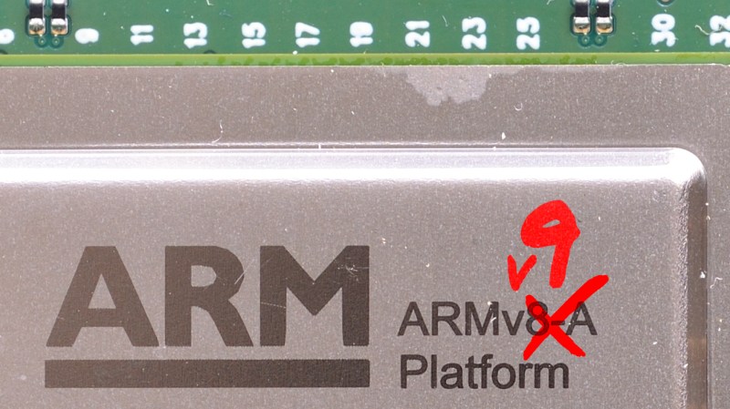
With ARMv7 being the first of the Cortex cores, and ARMv8 adding 64-bit support in the form of AArch64, what notable features does ARMv9 bring to the table? As announced earlier this year, ARMv9’s focus appears to be on adding a whole host of features that should improve vector processing (vector extensions, or SVE) as well as digital signal processing (DSP) and security, with its Confidential Compute Architecture (CCA).
In addition to this, ARMv9 also includes all of the features that were added with ARMv8.1, v8.2, v8.3 and so on. In essence, this makes an ARMv9-based processor theoretically capable of going toe-to-toe with the best that Intel and AMD have to offer.
Welcome to the High-End
It should be obvious that ARMv9 is not an ISA which we’ll be seeing soon in budget single-board computers (SBCs) like the Raspberry Pi and kin. The BCM2711 SoC of the Raspberry Pi 4, for example, uses Cortex-A72 cores, which implement the ARMv8-A specification. Since then, the ARMv8.1-A update added:
- Additional instructions for atomic read/write and more.
- Improved virtualization support (e.g. Virtualization Host Extensions).
- SIMD (vector) extensions.
In 2016, ARMv8.2-A added:
- Additional instructions for a variety of of tasks like half-precision floating point data processing.
- Scalable Vector Extensions (SVE): SIMD processing.
Followed later that year by ARMv8.3-A:
- Nested virtualization.
- Advanced SIMD complex number support.
The next three updates added and refined more functionality, creating an impressive list of required and optional updates to the base ARMv-8 specification. Not surprisingly, this large number of ISA specifications is a bit messy, and one of the things that ARMv9 accomplishes is bringing all of these versions together in one specification.
Another thing which ARMv9 adds over ARMv8 is Scalable Vector Extension version two (SVE2), the successor to SVE, and essentially the replacement of the NEON SIMD instructions. As Arm notes, the NEON instructions are still in ARMv9, but only for backwards compatibility. As the ‘Scalable’ part of SVE suggests, a major benefit of SVE over NEON is that it scales to the underlying hardware, allowing for even smaller, less powerful platforms to still handle the same SVE2-based code as a higher-end chip.
It’s telling that SVE has its roots in HPC (high-performance computing), with the Japanese Fugaku supercomputer being one of the first systems to make use of it upon its introduction last year. This means that ARMv9’s SVE2 will be very important for applications that process data which benefit from SIMD-based algorithms.
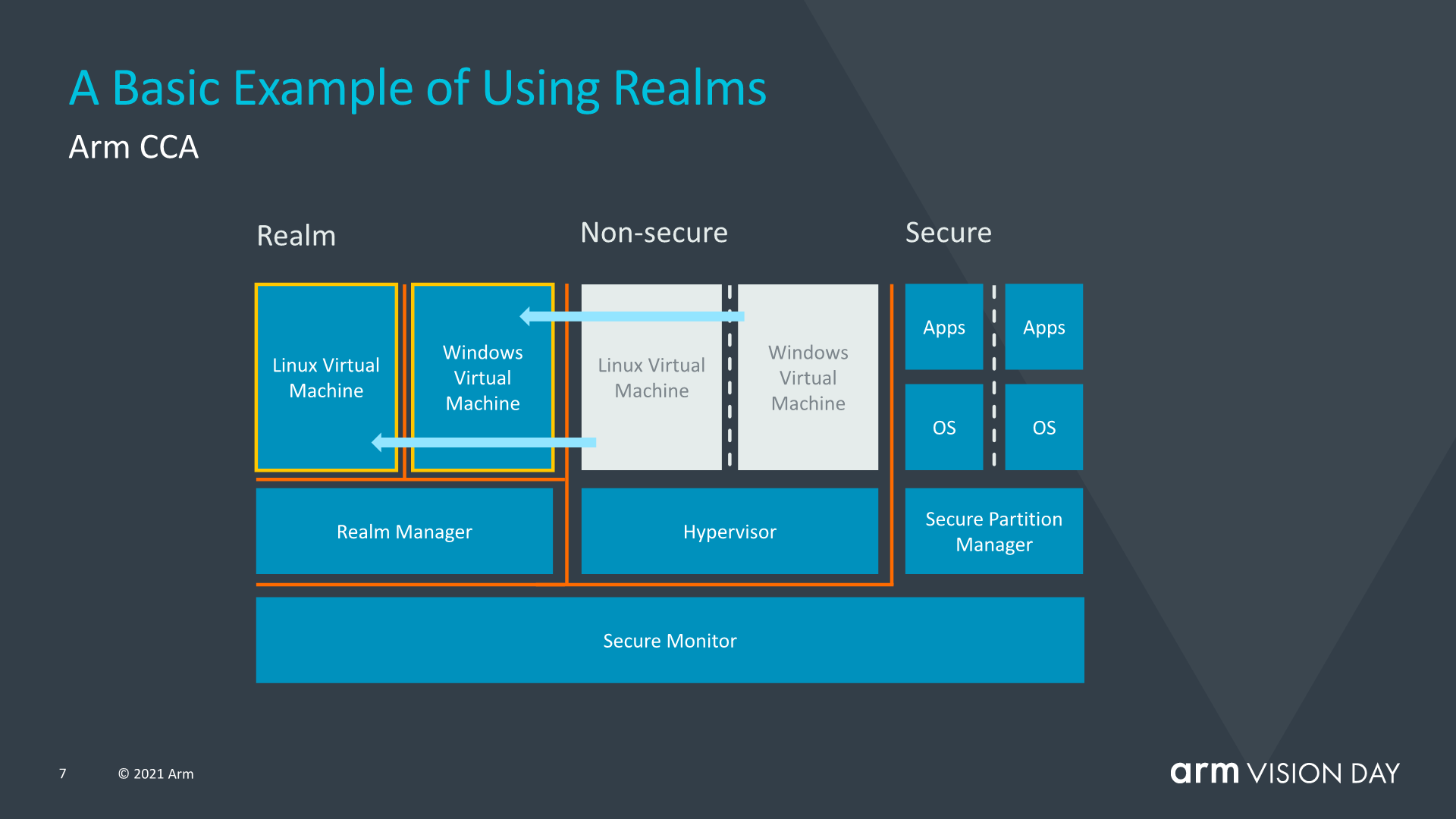
Realms and Tagged Memory
New in ARMv9 is the concept of ‘realms’, which can be considered as a kind of secure container in which code can execute without affecting the rest of the system. This works together with e.g. a hypervisor, with the latter handing a large part of the security-related operations to a new Realm Manager. The exact details of which aren’t known at this point, beyond the information which Arm made available at its recent announcement.
Not new to v9, but available since v8.5 is Memory Tagging Extension (MTE). Memory tagging is a mechanism to track illegal memory operations on a hardware level. This is similar to what Valgrind’s Memcheck tool does when it keeps track of memory accesses in order to detect buffer overflows and out of bounds writes and reads, except with MTE this is supported on a hardware level.
Having these features in the ARMv9 specification means that upcoming ARM processors and SoCs are likely to offer virtualization and security options that make them interesting for data centers and other applications were virtualization and security are essential.
Stay Tuned
Just a few days ago, Arm revealed the first two CPU cores which are based on the ARMv9 specification. These Neoverse V1 (“Zeus”) and N2 (“Perseus”) cores. Both of these are targeting data centers and HPC applications, with Amazon AWS, Tencent, Oracle, and other cloud providers likely to use them.
The low-down is that for in the near term, ARMv9 is something that the average consumer will have little if anything to do with as there’s not much incentive for many platforms to change even from baseline ARMv8-A to ARMv6-A. The need to license new cores and new IP is of course another factor here. All of this means that for the coming years, it’s not likely that we’ll see ARMv9-based silicon appear in mobile devices or new single-board computers. (Sounds kind of like a challenge for Hackaday readers, doesn’t it?)
That is not to say that it isn’t an interesting development, especially once ARMv9 with SVE2 and CCA ultimately do appear on those platforms. With massively improved SIMD performance — for example — many data processing and encoding tasks will suddenly become a lot faster, which could be a boon for anyone who wishes to daily drive an ARM-based system.
The ARM Ecosystem Today
As alluded to in the beginning of this article, the ARM ecosystem is relatively fragmented at this point, especially when one considers the highly popular Raspberry Pi boards and their simultaneous, continued use of ARMv6, ARMv7, and ARMv8, with middling support for AArch64 on the latter. Although it has its benefits to be able to use the backwards compatibility in ARMv8 and v7 for running ARMv6 (‘armhf’) binaries, it also removes a large part of the benefits of moving to these newer ISAs.
With 32-bit support in the world of Intel and AMD already firmly a thing of the past, it does seem rather quaint to hang on to 32-bit-only ARM ISAs, especially when simultaneously proclaiming the capabilities of these systems as a potential daily driver. Even just the 4 GB system memory and per-process memory limitations that come with a 32-bit architecture are sufficient to ruin a lot of potential fun there.
How long will it take before ARMv6 and ARMv7 will join ARMv5 into retirement? That’s not an easy question to answer at this point, even though the answer will likely play a major role in the answer to the question of how long it will likely take for ARMv9 to start playing a pertinent role outside of data centers.
A Note on MCUs
Amidst all this talk about server chips and SoCs, it’s sometimes easy to forget that ARM-based microcontrollers also use ISAs related to the Application profile ISAs. These -M (Microcontroller) post-fixed specifications have been updated over the years as well, with the Cortex-M55 using the ARMv8.1-M instruction set. This ISA adds the Helium vector processing extensions, adding significant SIMD capabilities to MCUs.
While the Application profile of ARMv9 won’t directly translate to the Microcontroller profiles in a feature-for-feature manner, any features which do make sense for an MCU platform are very likely to be translated to the latter in some fashion. Virtualization features for one do make little sense, but memory tagging as in MTE and further debug and monitoring features could be desirable.
When the first MCUs based on the Cortex-M55 appear over the coming years, this should give us a glimpse of what ARMv9 may bring in this area as well. Whether we will be programming those MCUs from ARM-based desktop systems by then is however still up in the air.


Although I can still buy (except for “chip shortage”) cortex-M0, the new processors from ST and the likes tend to be reasonably modern ARM cores.
If they aim for datacenter only use, then they can expect CPUs to sell for $1000+ Then that would allow a licencing fee that’s significant vs what people are willing to pay for a microcontroller. But once that licencing fee is low enough I expect to see a couple of years before we see reasonably small stuff also supporting ARMv9.
Nowadays I get an ARMV8 in my raspberry- and other pi’s right? A couple of years from now you get ARMV9 in that segment.
The embedded processors that I use are ARMv7 and never use the features beyond ARMv6. So the features not being strictly necessary is not an argument to not just implement the newer architecture in the newer chips.
Assuming Nvidia purchase of Arm get shoot down by regulators in various countries…
There is very little reason for Arm to drasticly increase their licensing fees as RISC-V and others might eat them for lunch for low end cores. They are almost giving the microcontroller Cortex cores out for free.
https://www.arm.com/why-arm/how-licensing-works
>Upfront Costs: $0 for the Cortex-M0, Cortex-M1 and Cortex-M3 CPUs
>Licensing: No additional license fee for the Cortex-M0, Cortex-M1, and Cortex-M3 CPUs
The old Cortext M would be in the high volume budget microcontrollers. The higher performances cores are likely be in the *microprocessor* lines as they are not stand alone parts – either require external DRAM or stacked DRAM die. Their minimum prices will be limited by their die size (+ DRAM cost) and won’t be in the same market.
Not sure about a couple of years for ARMv9 on dev boards, ARMv8 was announced october 2011 while the raspberry pi 4 was released in 2019. Other chips were faster, RK3399 releasing 2016 and hitting dev boards in 2017 (?). The S905 was early 2016 I think?
On the other hand the market has changed and there’s more interest in high performance ARM systems these days. I’d guess 5 years.
ARM designers: “RISC is finally taking its rightful place! Down with complex ISAs!”
Also ARM designers: *Adds every extension that x86 got over the last 20 years*
(Not saying it’s wrong or bad, just that it’s funny)
I guess you have to have a happen medium between pure RISC and CISC. Some things just need to be done in the hardware for speed and efficiency.
I know I dived into some assembly on the RPI4 loading the 64bit version of PI OS to learn ARM 64 assembly. Best way to learn is to ‘do’. I rather enjoyed it and the freedom of ‘lots’ of registers to work with over what I remember having to deal with on the z80, x86, and 680xx platforms.
68000 was very good about registers and its use for its time (being a CISC CPU). It had 8 data registers and 8 address registers (If I remember correctly one was used for stack), and you could use them freely, while on x86 and Z80 you had much less registers and, worse, they have special uses: some operations only work on specific registers: it was a nightmare we get used to.
ARM has though been a CISC architecture for a very long time….
It isn’t much RISC left in it.
And even RISC-V is likely heading down the same street sooner or later.
Implementing more application specific instructions does increase both peak performance and peak power efficiency.
Though, CISC tends to have higher idle power consumption, even if this can be circumnavigated to a degree with various low power states where one deactivates certain features, though at the deficit of not having the feature in that state. (One can get the feature back with microcode while still being in the low power state, but this is its own can of worms….)
But there is technically more to the RISC/CISC definition than just instruction count, or even instruction complexity.
How the instructions interfaces with memory and IO also effects what camp the architecture belongs in.
Though, in the end, stepping outside or RISC is really trivial.
Just have a couple of instructions working directly on memory (that aren’t fetch/store instructions), and go past 40-60 or so instructions and it is CISC.
But some people consider RISC more of a design philosophy, where one aims at simplicity in instruction calls and memory/IO structures. So to a degree ARM is somewhat still RISC. (Or at least that is what I think when I work on one of my own “RISC” architectures that clearly has strolled far, far into CISC territory….)
Is it maybe more helpful to say e.g. load/store architecture (or stack-based architecture, etc) instead of RISC, if that’s a key enduring design difference beyond “reduced”?
RISC tends to be load/store, but it isn’t a strict requirement.
And to be fair, a RISC architecture can have no load/store instructions at all. Ie, an architecture without any registers that instead only works directly on memory.
Being load/store is pretty much the defining characteristic of a RISC style ISA. One of the original arguments behind the RISC movement was that any instruction being able to access memory, especially making multiple accesses, significantly complicates the hardware.
An ISA that only does memory-memory operations (e.g. TMS9900) would most decidedly be CISC.
Bit.
Yes, load/store is a common feature of RISC.
But if an architecture lacks registers (other than the program counter and state flags), then it can’t do load/store, since there is nowhere to put that data. But if the architecture is still adhering to the other rules of the RISC philosophy, then it is arguably still RISC.
For an example, we could take the ARM core, rip out the registers and append an address onto our instruction call for every register that we would have needed. The architecture would be fairly equal from a complexity standpoint. (Downside is the extra bandwidth needed in our memory/cache systems, registers are common as mud among architectures for a reason.)
We could make an even simpler architecture, where every instruction call consists of an up-code followed by 3 addresses, two input terms and an output. This can be kept the same for all instructions including conditional jumps and bitwise logic operations. Having hardware pointers would be a saving grace, but lets not add complexity. The architecture would be RISC (as long as our instructions count isn’t huge and aren’t taking more than 1-2 cycles to execute), but it lacks registers and therefor isn’t a load/store architecture.
But even then.
A lot of RISC architectures do break rank and does have instructions that bypass the whole load/store idea. This is generally though avoided, but if there is enough of a performance improvement, it can be a worth while thing to include.
Though, to be honest, the whole RISC/CISC debate is fairly polarized, or one sided. Since everything that isn’t strictly RISC tends to be branded as CISC. Unless the architecture has a history of being RISC, then it can be labeled RISC even if it is has drifted clearly into the CISC category.
But then we have the people saying that modern x86 processors are RISC “under the hood”, even if this is laughably incorrect in practice. Since x86 has a fair bit of more nuanced instructions that would take too many cycles to execute via microcode, simply stated, the throughput is too large for it to be an emulation running on top of a RISC core. (Not saying that one can’t emulate x86 on a RISC core, but for peak performance and power efficiency under load it isn’t practical. The Intel Atom might though be “true” RISC under the hood, due to it’s low performance and low idle power consumption nature. (RISC tends to win at idle power consumption, why it is perfect for mobile applications, and other applications that are mostly idling and running on batteries.))
In the end.
If an architecture is RISC or CISC isn’t a binary option, there is a fairly large fuzzy boarder between the two: But CISC do make up the majority of the spectrum, since there is no real upper limit to complexity.
Another worth of mention RISC trait (and maybe its bigger advantage over x86-64) is the fixed length instructions that allow to build very simple decoders.
E.g. a huge x86 core like Zen sports a mere 4-way decoder while a mobile core like Apple Firestorm has a whopping 8-way (only POWER 10 at the moment matches it) with a ~630 instruction deep ROB.
M1 so far is the odd ball, so shouldn’t be used as a generalized example. The rest of the Arm chips only have 3 or 4 width decoders. see wiki under “Designed by ARM”
https://en.wikipedia.org/wiki/List_of_ARM_microarchitectures
Apple business model is actually kinda like consoles, as they are vertical integrators operating differently than traditional chip vendor, OEM integrators. They can and are throwing hardware at the problem. They achieve low power and very good performance via massively parallel at low clock frequency.
The fixed instruction does make it easier. BUT when you compared it to the extra chip space/complexity for the extra execuion units, it is a small overhead.
saidone.
Though, the comparison of 4 vs 8 instructions decoded per cycle is partly also missing the difference between RISC and CISC.
The 4 instructions decoded by the CISC processor can produce a far more complex workload than the 8 instructions in the RISC one.
We also need to consider what our instructions are doing when making the comparison.
Though, for workloads that aren’t optimized for the CISC architecture, but instead relying on its simpler instructions, then the RISC based architecture will tend to have an upper hand since it is easier to optimize for due to having fewer instructions for one to decide between. (Especially if one wants backwards compatibility to older processors.)
But to be fair, I can beat the world’s best boxer if I tie their hands behind their back and glue them to a wall. (It isn’t a fair fight.)
Or I can benchmark a QUDA only workload on an AMD GPU and conclude that AMD’s GPUs are trash compared to nVidia, but this too is flawed. (except if one is looking to just run that workload and don’t feel like reprogramming/porting it.)
A comparison in performance and efficiency needs to show the best side of both.
Ie, our application needs to have some effort spent on optimization on both platforms for the comparison between the platforms to actually state anything useful.
But even CISC architectures can have fixed instruction call length and still be CISC.
And a RISC architecture can have variable instruction length and still be RISC. (Although a bit less RISC than if it were fixed, due to the added complexity.)
The main reasons for why one isn’t always spending more effort on increasing decoding speed is due to other factors in the larger system already being bottlenecks. Ie, a faster decoder doesn’t give any benefit and those resources can instead be spent on the actual bottlenecks in the system.
For both RISC and CISC architectures, one of the bigger bottlenecks to peak performance is the interconnect between memory and the CPU, cache somewhat fixes this issue, but cache have bandwidth limitations as well.
CISC has the advantage that it needs less code to execute the same workload as a RISC architecture, generally speaking that is. But a lot of RISC architectures have smaller instruction calls in general. Not to mention that it is common among RISC architectures to use microcode to compress common tasks into single instruction calls. (The decoder is though translating, but the RAM and cache is non the wiser.) So these two things does close the gap a bit between RISC and CISC in regards to memory intensiveness. But depending on the CISC instruction, the difference can still be large.
But I also do have to point out.
The “4 way” part you mentioned in regards to AMD’s Zen architecture is the L1 Cache.
Ie, it can work on 4 cache lines per cycle, either writes or reads. A given cache line typically contain more than 1 instruction call. The size of a cache line can vary, but anywhere from 8-64 bytes isn’t uncommon.
And Zen 3 has an 8 way L1 cache as well… So that isn’t particularly unique to RISC. (Though, the cache implementation is fairly free from whatever ISA one uses, though the ISA can have certain expectations that one generally should live up to.)
> the comparison of 4 vs 8 instructions decoded per cycle is partly also missing the difference between RISC and CISC
I’m not talking about the density, but the feasibility of a wider decoder. Of course either Intel or AMD would make a larger decoder if they could.
> The “4 way” part you mentioned in regards to AMD’s Zen architecture is the L1 Cache
No: I mentioned the instruction decoder, not the cache.
> And Zen 3 has an 8 way L1 cache as well
Seem that you’re confusing the instruction cache with the instruction decoder that are two completely different entities, hope this diagram will help:
https://en.wikichip.org/w/images/f/f2/zen_2_core_diagram.svg
Cheers,
Marco
P.S.
The “8 way” related to the cache does not indicate the wide of a data path or number of ports but rather the cache placement policy.
I would say rather than RISC, it is now just a 1-address architecture versus 2-address. Or what the vocabulary deprived call a “load-store architecture” for some reason. Plus ARM never had enough registers to fit among the RISC crowd (PA-RISC had 32/64, SPARC is 72 to 640, Berkeley RISC is 78, SGI had 32 64 bit registers and 32 floating point registers).
Anyway, the early ARM is a 32 bit 6502 (of course) with more registers. The instruction set is great and writing efficient code is easy. The amount of stuff that a single instruction can do in a single clock is pretty darn impressive yet not complicated to use in assembly. Good times. VLSI ARM7500 board from 1994 top image here http://www.regnirps.com/Apple6502stuff/arm.htm
“a 1-address architecture versus 2-address.” is interesting.
I have personally designed some hobby architectures using 2 source addresses and 1 store address per instruction. All though a bit clunky….
And yes, RISC architectures tends to benefit from having a lot of general purpose registers, makes it easier to implement code without having to worry as much about the data getting flushed away in cache, or collide with other data if using global variables for data storage.
But there is a downside with registers, one needs to offload their content on a thread switch. The thread itself will already have some amount of data associated with it as is, but with every new register, that dataset gets larger and takes more time to store/fetch. (This is however fairly minior in the larger scheme of things, and SMT makes this even less problematic. Unless one worries about it eating away fractions of a % of one’s memory bandwidth.)
Another downside with registers is handling their content and switching it to our various hardware functions, especially if we start doing out of order execution, then things can get messy.
Though, you missed PowerPC on your list, having a total of 64 registers. Half of them being float ones.
And yes, it is fairly impressive what one can do in a single clock cycle when having dedicated logic for the function. Though, at other times, one can need a clock buffer or two for stability, adding additional cycles to the operation. But generally speaking, one will tend to want to spread out the load, execute and store into individual cycles regardless. And with out of order, one tends to also want a queue somewhere around the load stage.
Indeed, I completely forgot PowerPC! Maybe because I never actually wrote anything low lever for one. And Linux users owe Device Tree and Open Firmware/Open Boot to SPARC and PowerPC Apples.
And I agree, out-of-order and pipeline tricks and context switching can take out the linear fun. In fact I avoided the Thumb set because of the way it diverged from the basic rules. I implemented a very traditional Forth on the ARM7500 and it was very fast and smooth. I recall that I found stacks so easy to use with stack pointers in registers that aside from a floating point stack I added several more to isolate things that normally were stuck on the return stack. Hmmm, a loop stack I think and, drat. Now I have to find the source code!
Forth is rather straightforward to do a classic threading implementation with enough registers and the right addressing modes. I implemented one on a 6809 back in the mid-80s because the inner loop was literally two instructions, and the U register was the data stack pointer.
Found the old assembly code. The Forth inner interpreter, NEXT, is two instructions so it is in-lined in most places as a macro. The stack pointers are as above. There was a significant increase in performance with the tops of the stacks in registers with 2 registers for the floating point TOS.
Yep, designed as a Mini, turned into a Hummer.
The RISC as proposed by Hennesy and Patterson does not forbid more instructions. Instead, it simply requires justifying every instruction by detailed quantitative analysis: new instructions have to be faster than their implementations put together with existing simpler instructions, but more importantly, the complex instructions cannot slow down the entire design, by e.g. introducing pipeline hazards or complex unwinding schemes.
So, if a complex instruction can be shown to help the overall design, it’s an entirely acceptable RISC.
This is a good summation of the RISC philosophy.
It is a very common misconception “Reduced” in RISC means reduced number of instructions. While a lot of RISC have less instructions than some CISC, it is not always true. For example PowerPC had more instructions than some CISC (and there was the joke it was “Complex RISC”).
The correct interpretation about “Reduced” in RISC is a reduction in instruction complexity. That is instructions themselves are simpler (load-store model) than in CISC.
In CISC you have all type of instructions varying from simple to very complex, from short to long, while on RISC all are reduced/simpler.
Are there any existing ARM based desktop base units or laptop computers or even just an ARM motherboard that support say 16, 32 or even 48 GiB of RAM that can run an Open Source Operating System, maybe with a few SATA ports and couple of actual USB 3.0 ports (not a USB hub chip) with at least gigabit Ethernet ? At a reasonable price, basically a computer without an Intel Management Engine (IME) or an AMD Platform Security Processor (PSP).
And do not even suggest an Apple M1, because the graphics processor is not using industry standards. Work is ongoing, even with the major limitation of no documentation ( https://github.com/AsahiLinux/gpu ).
There’s someone on eBay selling ThunderX2 32 core 1.8GHz motherboards and CPUs for $999.
Eight DIMM slots, 1 PCIe x16 slot, 1 PCIe x8 slot, four SATAIII connectors. Ethernet, USB 3
Thanks, I did not think to look for ARM servers, gigabyte even ship a few motherboards with ThunderX2 cores via third parties ( https://www.gigabyte.com/Enterprise/ARM-Server )
That ThunderX2 chip reminds me a lot of the UltraSPARC T1 (from 16 years ago) or T2 or any of the later chips in that product line, which were designed for maximum multi-threading performance, it is a real shame that Oracle killed off SPARC hardware.
Making your own processors had turned into the superpower arm race. It was getting so expensive that few can afford to do and may bankrupt themselve doing it. Intel might turn into an investment company if they decoded to quit chip business… :P
Pooling R&D + production volume is the business model behind fabs and commodity parts.
The “reasonable price” bit basically requires a couple of generations of demand-driven price reduction in an existing market. At the moment, the market for ARM has been generally limited to either high-end specialist hardware, or low-end non-general-purpose hardware. Just like there’s no inherent reason you couldn’t have an OpenPOWER design for cheap, except that there’s not enough market at current prices to pay for the production streamlining that would be needed to bring the prices down.
The Apple M1, although it won’t fit your requirements directly, at least is demonstrating convincingly that “a reasonably architected ARM can indeed have compelling cost and performance advantages”. Maybe that will translate into enough market interest and competition to drive a low-cost general purpose system, and maybe it won’t. I’m personally aware of at least two different companies with internal manhattan projects trying to achieve this, so there’s at least some interest.
It is sad commercial ARMs usually are not very good commited to the open model. Open and privacy projects based on ARM hard have very limited options. For example Librem 5 and MNT Reform choose NXP because it has much better support and documentation than normal comercial ARM (I suppose it is derived from it is more industrial focused), and it has the most open soft model on modern commercial ARM I have heard of. MNT Reform doesn’t comply your requirements: only 4GB of RAM (and only 4x ARM Cortex-A53 low performance cores).
If you want more openees friendly, less closed parts, I think today you must look outside ARM. For example RISC-V HiFive Unmatched board, but Linx support isn’t complete, it is expensive and only support 16GB RAM.
Other option is POWER ISA, now totally open. For example with this motherboard and IBM POWER9: https://hackaday.com/2018/11/26/a-sub-1000-non-x86-motherboard/
If you want go without IME, AMD PSP, ARM blobs, etc, you have few options, and they are not very cheap.
Minor correction. “Fukagu” should be “Fugaku”. This is another name of Mt. Fuji.
Methinks thou hast misspelled the name of the Japanese computer.
B^)
That was a good spot “Fukagu supercomputer” (wrong) should be “Fugaku supercomputer” (right).
Neoverse V1 is not Armv9-A but Armv8.4-A, so far the only confirmed v9 core is Neoverse N2.
It will be interesting to see how many servers end up shipping with V1 cores now that Armv9 has been announced, and which of the coming client CPU cores from Arm, Apple or others are going to include the SVE2 instructions. In theory there could be a single core design with implementations choosing either Armv8.5-A without SVE2 or Armv9.0-A when SVE2 is included.
“The Management Engine started to appear in Intel computers around 2007. […] AMD computers made after 2013 also have a separate computer within the computer, called PSP (Platform Security Processor), which has similar issues.”
What about armv6, armv7, armv8 etc. Since when do ARM processors include similar co-processors or hardware trojans? Looking at the success of RPI and similar platforms it seems almost like a no-brainer that such backdoors are certainly included. Any new research on the topic?
The original article about IME https://www.fsf.org/blogs/sysadmin/the-management-engine-an-attack-on-computer-users-freedom
1) RISC term is not technical, but marketing one. Almost pure “RISC” processors were developed before that term was coined.
2) Instructions are “Reduced”, not the “Set”. It means that architecture is Load-Store and there are no complex microcoded instructions. That requirement was relaxed a little.
3) Almost every new architecture is “RISC”-like (we have to decouple memory load from data usage), but it is a pragmatic characterization, not dogmatic.