We all remember the litany from various math classes we’ve taken, where frustration at a failure to understand a difficult concept bubbles over into the classic, “When am I ever going to need to know this in real life?” But as we all know, even the most esoteric mathematical concepts have applications in the real world, and failure to master them can come back to haunt you.
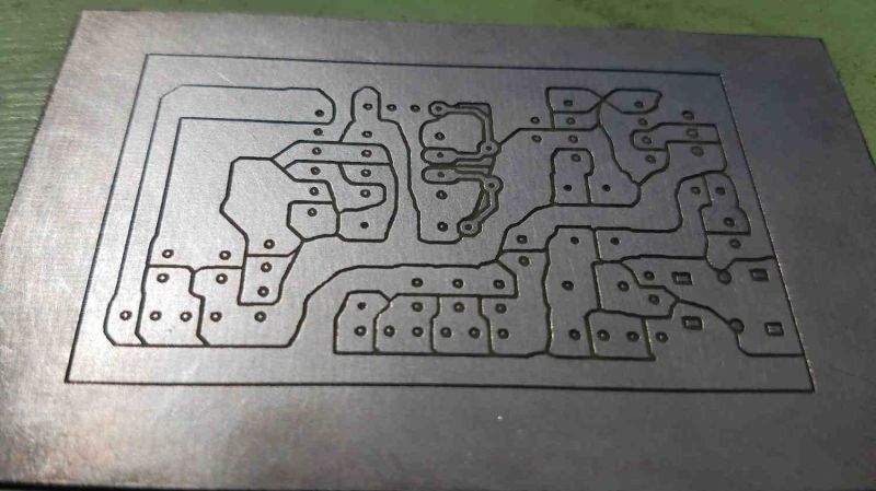
Take Voronoi diagrams, for example. While we don’t recall being exposed to these in any math class, it turns out that they can be quite useful in a seemingly unrelated area: converting PCB designs into easy-to-etch tessellated patterns. Voronoi diagrams are in effect a plane divided into different regions, or “cells”, each centered on a “seed” object. Each cell is the set of points that are closer to a particular seed than they are to any other seed. For PCBs the seeds can be represented by the traces; dividing the plane up into cells around those traces results in a tessellated pattern that’s easily etched.
To make this useful to PCB creators, [Craig Iannello] came up with a JavaScript application that takes an image of a PCB, tessellates the traces, and spits out G-code suitable for a laser engraver. A blank PCB covered with a layer of spray paint, the tessellated pattern is engraved into the paint, and the board is etched and drilled in the usual fashion. [Craig]’s program makes allowances for adding specific features to the board, like odd-shaped pads or traces that need specific routing.
This isn’t the first time we’ve seen Voronoi diagrams employed for PCB design, but the method looks so easy that we’d love to give it a try. It even looks as though it might work for CNC milling of boards too.


Does anyone know of a similar application that works on a vector format PCB rather than on raster images? I am routing my PCBs on a CNC machine so my workflow is Gerber -> isolation -> NC code. This works fine but traces and pads have too much detail. If I could reduce the complexity of the isolation vector format using Voronoi diagrams it would significantly cut down the routing time.
It is a flag:
pcb2gcode –voronoi
https://github.com/pcb2gcode/pcb2gcode/wiki/Options:-Milling
There is also a flag that also includes height-probing macros for linuxCNC gcode…
bCNC of course also does this probing cycle too.
The only pain when we tooled up was compiling a version of pcb2gcode that didn’t seg fault ;-)
Cheers,
J
Yes, I built a tool that does precisely that:
https://github.com/abetusk/gbr2ngc
It doesn’t do Voronoi regions but rather does polygon boolean operations (via the library clipperlib) and polygon offsetting, if desired, to account for the endmill radius.
gbr2ngc is fully RS-274X compliant though you should always be looking out for bugs.
Visolate: https://github.com/Traumflug/Visolate
Milling Voronoi patterns is all but new.
The OP cites Visolate as inspiration in this GitHub README.
https://github.com/micsche/kicad-laser-min
Nice. It looks like it has a side effect of minimizing the tool path length at the same time. Handy.
But good luck drilling those holes on center. The drill is going to want to walk into that gutter.
A good update would be to put a center starting hole in the middle of the intended through-hole.
Totally agree about the through hole marking as a single dot instead of a circle
Had the same thought.
Someone needs to invent a CNC center punch.
One should drill at least pilot holes using CNC as well. For doing this, regular PCB milling applications are just fine. I typically drill 0.75mm and 1.00mm by CNC, this cover like 90% Then enlarge the bigger ones manually. Drilling like 250 holes manually is a chore.
Man…. Why even bother wasting your time when PCB costs are so cheap nowadays.
Yeah. Why even bother reading Hack-a-day when Hello magazine is online nowadays?
But they’re really not once you add shipping charge (min $15+).
Then a week+ waiting time.
For each iteration.
You can easily blow $100 and a month of delay using china boards, vs a day or two diy.
Maybe you want to etch in your own back yard and not outsource to China?
COVID makes shipping logistic much more unpredictable. I can get away doing toner transfer usable for TSSOP chips with bare minimum efforts, cost and get boards made the same day at my own home.
Why even wasting my time waiting for a pcb to be delivered when i can finish it before you ate your lunch ?
I would have liked my profs to explain math with interesting application examples instead of (mostly) showing how cool (wir hey think) they are dealing with super abstract ideas…
shipping from CN to EUR has never been so fast, in fact it’s the domestic part in EU that is 3/4 of the time…
Spell check… it should be “(they think)”…
This is for casual use and low requirement non-critical circuits.
If your application requires you to control the width and shape of PCB traces, then this is not what you want. e.g. Analog grounding, PCB traces for current measurement, capacitance sensing, high speed circuits, controlled impedance, RF application where the traces are used as antenna, inductor etc.
Just doing “flood fill” (while leaving boundaries intact) everywhere that’s empty would accomplish the goal of reducing the amount of etching required. The traces would be left alone, so their lengths and thicknesses would not change.
I don’t think tessellated means what you think it means.
It must be hard to solder without thermal pads!
I was about to say the same thing. Some of those traces are going to be a nightmare to heat.
pcb2gcode –voronoi –preserve-thermal-reliefs
Even without thermal reliefs a 1oz copper PCB is a breeze with a 25W iron, but 2oz needs a 60W to 100W iron.
The 3 second rule has always been true, in that if you can’t finish the joint with a nice fillet in 3 seconds you are using the wrong equipment. As cooking the joint with a small iron often causes a lot of damage to the PCB/parts.
;-)
even the most esoteric mathematical concepts have applications in the real world
Hahaha nope
Sounds like a lot of effort for what could be just a lowpass filter done with a lens and some cardboard.
For more disastrous tips, follow me on MySpace.
What impedance are those pcb tracks I wonder, 0.01 ohm?