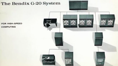
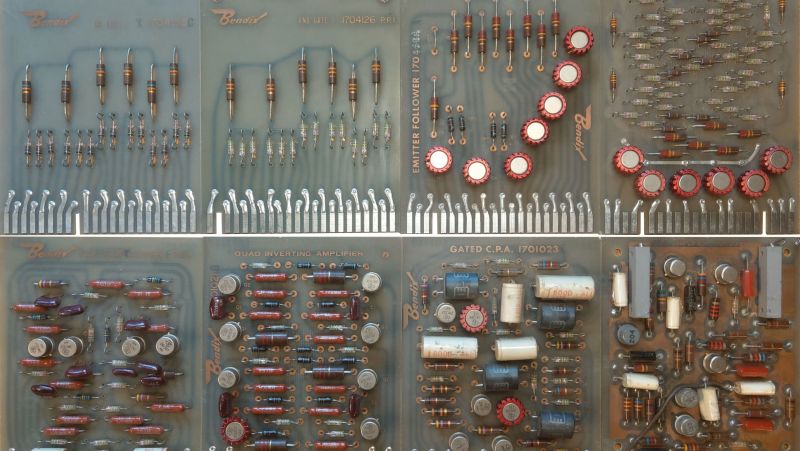
[David Lovett] aka Usagi Electric is taking a dive into yet another old computer design, this one from the early 1960s. He recently obtained eight mystery circuit boards on-loan for the purpose of reverse engineering them. It turns out these came from an old mainframe called the Bendix G-20, a successor to the 1965 G-15 vacuum tube model. The cards are:

- Full Adder
- AND Gate
- OR Gate
- Emitter Follower
- Flip Flop
- Quad Inverting Amplifier
- DLO Amplifier
- Gated CPA
Most of these are pretty straightforward to figure out, but he ran into some troubles trying to understand the full adder board. The first issue is there is some uncertainty surrounding the logic level voltages. This system uses negative voltages, with -3.5 V representing a logic 1 … or is it a logic 0? And even taking into account this ambiguity, [David] is having a hard time deciphering how the adder works. It uses a bunch of diodes to implement a logic lookup table of an adder — except he is not able to make it match any known addition scheme. [David] has called out to the community for help on this one, and if you have any ideas how this adder works, visit his wiki linked above for more information and give him shout.
We don’t know how [David] squeezes in the time for these side projects, when he is so busy on the Centurion mini-computer restoration and the monstrous single-bit vacuum tube computer he is building.


I wonder how much he could have worked out just from high resolution CT scans of the circuits?
We often think of the full adder being implemented using XOR and AND gates. However, it can be expressed in Boolean equations that reduce to the AND-OR-INVERT structures that were provided by the diode transistor logic (DTL) used in the Bendix G-20.
I found a logic diagram of the classic 7480 TTL adder, which shows the full adder implemented in this manner.
https://makeyourownchip.tripod.com/7480.html
The diodes in the emitter follower could be filters or signal condition.
Heh, that board format looks familiar, like I got some in a batch of “boards for component reclamation” from a surplus house in the 90s. No idea where they went though, moved 3 times.
Nice stuff! Looks like it has complementary in- and outputs (1=!3, 2=!4, C=!D, and B=!E, A=!F). 1+2+C are inputs, B is sum, and A is carry. Pretty much a discrete PAL. Does this make sense? No clue though why the two carry ins are both inverted and not just swapped.
I’m sure the author knows, but these old discrete logic circuits don’t always have a single logic convention. Some bits in the word may be active high and others active low, depending on the circuit before and after them. This can obscure the adder function.
The transistors in the “Emitter follower” schematic have collector and emitter swapped. As shown, the emitters are tied together (common emitter configuration). An emitter follower circuit is common collector.
It is possible to swap emitter and collector in some applications, but the results are usually quite inferior.
It could be a mix of Resistor-Transistor-Logic (RTL) and Diode-Transistor-Logic (DTL) and tricks to save component count with NOR versus AND OR and “look up” with diodes, etc. I would plug the circuit diagram into any of the simulators and feed it inputs to generate a truth table. Or do it live with a multi-channel scope.