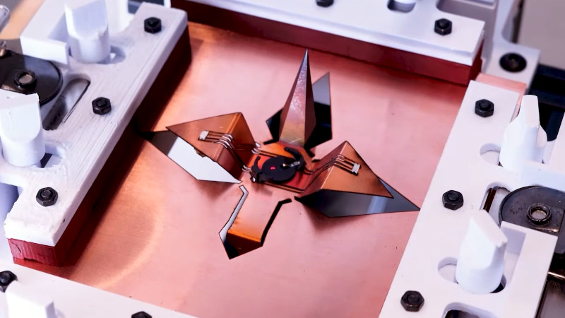
It’s not often we feel that something we’re featuring is a genuinely new and groundbreaking technique, but a team from the University of Maryland’s Small Artifacts Lab may have done just that with their foldable and flexible PCBs created using a fiber laser engraver.
Laser engraving a PCB is nothing new, but they’ve taken a custom PCB material made using Kapton tape and copper foil, and fine-tuned the engraver to not only selectively remove copper, but also to create in-place folds in the Kapton substrate. They have even used the laser to melt solder paste and solder components, though we’re not so convinced about the quality as seen in the video below the break. This means that they can not only create 3-dimensional PCB sculptures but also useful structures such as their example of an all-PCB micro switch. To make things easy they’ve even created a custom CAD package for designing in this medium.
Perhaps best of all, there appears to be nothing here that couldn’t be also performed outside the lab by anyone with enough Kapton and copper, and a fiber laser. We’re looking forward to where this technique will go. If you’re interested, you can read their paper here.


“Fiber” laser only marginally describes the laser technology used. It just points that the light produced by the laser unit travels in an optical fiber to the tool head. The more correct designation is “fiber-coupled” laser.
The linked paper does not provide any information either.
maybe it´s a 1064nm (infrared) DPSS laser pump, but don´t know for sure. The optical power used is also not mentioned.
You appear to have your definitions precisely backwards.
A “fibre-coupled laser” is just a laser that’s optically bonded to the end of an optical fibre to direct the laser light to it’s destination.
A “fibre laser” is a laser which has an amplification stage that occurs inside a specially doped fibre that is externally pumped. The fibre is not simply a means for transporting the laser energy, but is a critical part of the laser assembly itself.
It is clearly stated on page 3 that “Our work and experiments are based on an off-theshelf 50W desktop fiber laser engraver [6] as is shown in Figure 1a.” Try actually reading the paper before making uninformed comments.
As pelrun commented below, you also totally misunderstand the concept of a fiber laser. Suggest you read up on the background to them: https://en.wikipedia.org/wiki/Fiber_laser
mea culpa, one learns every day
Very interesting, and certainly usable for prototyping but I’m not convinced its a good method really. Seems like a great excuse to play with laser though and who knew a pasta machine has use in a lab!
I could see it being useful sometimes, but on the whole it seems like the worst approach to using a laser for a PCB, the ol’ laser off the etch resist seems to be substantially better in end result. Perhaps better work holding (vacuum hold down table perhaps) and refinements to this technique could get it there though, and its always very hard to judge such things just from images – you just don’t have enough reference scale to know if the bits making you dubious are large scale or tiny scale flaws – is that part/trace for a grain of rice SMD? bigger? or a really tiny SMD part? Really needs the side by side comparison to the same parts via other methods.
As an origami fan I have mixed feelings on kirigami, its always felt like cheating, but no denying its a good look.
Really fascinating stuff! Thanks for posting.
Very cool. They did a great job of exploring several of the basic “rules of design grammar ” so that others could effectively apply them for future applications.
Very much enjoyed the video. I would love to see a board with Kapton on both side of the copper. This could be a great tool to have in the shop. Anyone got a five grand to buy me a laser?
The only interesting information I got from it, is that I could “theoretically” make a lightburn file to laser solder legged parts on my pcbs (after stencil and placement of course), instead of throwing the board in the oven 😅
Very cool. They did a great job of exploring several of the basic “rules of design grammar ” so that others could effectively apply them for future applications.Very much enjoyed the video. I would love to see a board with Kapton on both side of the copper. This could be a great tool to have in the shop. Anyone got a five grand to buy me a laser?