We’ve taken ICs apart before, but if they are in an epoxy package, it requires some lab gear and a lot of safety. Typically, you’ll heat the part and use fuming nitric acid (nasty stuff) in a cavity milled into the part to remove the epoxy over the die. While [100dollarhacker] doesn’t provide much detail, he appears to have used a Tesla coil to do it — no hot acid required.
Initial results were promising but took a long time to work. In addition, the coil gets very hot, and there is a chance of flames. The next attempt used a 3D printed cone with a fan to push the plasma over the chip. The first attempt shorted something out, and so far, each attempt eventually burns out the MOSFET driver.
We are always interested in the practical uses of Tesla coils and what’s inside ICs, so this project naturally appealed to us. We hope to see more success reported on the Hackaday.io page soon. Meanwhile, if you have a coil and an old IC lying around, try it. Maybe you’ll figure out how to make it work well and if you do, let us know.
The easiest chips to open are ceramic packages with a gold lid. Just use a hobby knife. There are less noxious chemicals you can use. If you want to use fuming nitric, be sure you know what you are doing and maybe make some yourself.


Pliers work just fine. CO2 laser as well.
Pliers with hot air works fine but not for all chips. For example it’s a fail 100% of the time for Sanyo. And it usually fails for Mitsubishi, Hitachi, National semiconductor. Also hard to use with Motorola.
Laser don’t work. It destroys the silicon. It seems ok until you look at the chip under the microscope.
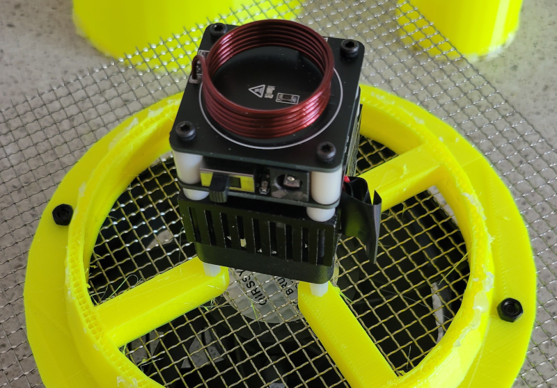
It’s useful from the backside so you can locate the paddle (or the die because sometimes there is no paddle).
I think that some special lasers make it possible to not damage the silicon, but it’s not really something accessible.
This is a really ingenious idea. I wonder if a plasma cutter used for metal fabrication would be a good alternative, as it provides plasma and air flow.
It creates that plasma by melting the target metal with high amperage electric current… You wouldn’t be left with a usable chip even if you could strike an arc on the epoxy (which you can’t, it’s nonconductive) and even using some sort of sacrificial conductive layer on top would deposit slag everywhere.
Technically the flame from a cutting torch is plasma too, but you would have the same issues with slag in addition to heat control.
This is firmly in laser territory!
We had a test stand for testing circuit boards that used the MACH2XX family of chips. For some reason someone decided to rewire it (apparently after hours and did not fess up to it) and got the power wires crossed which turned it into a depackaging machine instead. In a couple of seconds it would blow a perfect inverted cone out of the top of the chip allowing complete access to the chip and wires. They must have destroyed a dozen or so chips like this before they realized what the real problem was and fixed it.
Gas stove + pliers work also. Even just gas burner does. Either heat it up until the epoxy turns rubbery (then it’s time for pliers), or burn the package all together, the silicon will survive. Guess Tesla coil will damage the circuitry first. Acid allows die access without damaging the chip, sorta brain surgery. All the other methods are destructive.
I have tried stove method it was not successful at all especially for small ICs. Why do you think Tesla coil will demage the circuit? Anyway, the idea is to decap and look on a ICs never tried to operate it.
The coil could induce AC, at voltages and/or current, that would fry the delicate circuitry. That’s my guess anyway.
The best method if you don’t want to damage the die is hot air + pliers. But it don’t work for all chips.
Burning the package destroys the chip, but it’s only visible under the microscope. The silicon will survive but not the passivation / metal. In the best case you will have a lot of discolorations and only minor damages on the passivation layer. In the worst case metal will not be readable at all.
In short, it’s a bit of a last resort solution.
Has anyone tried a CNC mill to remove the top with 0,05mm layers?
CuriousMarc has done this in at least one of his videos. AFAIK it wasn’t CNC, might have been a manual Bridgeport.
“… managed to remove epoxy from Atmel’s Attiny85.”
Was that from the Attiny85 he was using to control the tesla coil?
No, the circuit used is detailed in https://hackaday.io/project/191435-tesla-coil-scientific-way. No digital components there.
Some epoxies will be greatly weakened by hot acetone. There’s a fire/explosion risk, but I’d rather deal with acetone than a strong acid.
Another option is grinding off the epoxy.
Sorry if I sound dumb, but wouldn’t X-rays be the easiest way to see inside without destruction?
X ray is is one of the techniques but you need special equipment, while here you can use simple(metallurgical) microscope. I use OpenFlex.
The resolution of X-ray equipment is generally far too low to make out the sub micron features on even older IC chips. This is not to say that X-rays can’t resolve to that level because of their wavelength; they have a shorter wavelength than visible or UV light. But lenses for X-ray systems are not as simple as precisely ground and polished glass. You can see the bond wires and lead frame. This is neat but not very useful if you are tring to look at the structures on the chip. Also a commercial X-ray system tomography system with anywhere close to micron resolution runs onto the hindreds of thousands of dollars. But you could probably DIY one for half that if you have access to a well stocked lab and macine shop and a few years to spare
Years ago I had to reverse engineer some 20X10 PALs. I ground down the epoxy till I saw the bonding bumps on the die. At that point I hit it lightly with a torch. Took an Xacto knife and scored around the perimeter of the die. When I was against the edge of the die I just flipped the remaining epoxy off of it. Then I could read the condition of the fuses.
What about using MOSFETS from the CCCP
Using a fan with a cone requires careful design. The problem is that the air coming from a fan isn’t moving in a straight line, but rather it’s spinning in a vortex. If you send spinning air into a narrowing cone, it will want to spin faster, and centrifugal force will want to push the air towards the larger part of the cone, thus slowing down the forward movement, possibly even reversing it.
Adding a couple of perpendicular sheets in the cone that are parallel to the desired airflow can help negate the spinning, though there are probably other good solutions as well.
I have used hot sulfuric acid on glass-filled epoxy packages by building a teflon (PTFE) block as a holding fixture fitted to a glass tube immersed in a flask of acid heated electrically. The acid is drawn through the tube by a vacuum generated by a standard lab-type water eductor on a side passage in the teflon block. The effluent is diluted by the water and flushed down the drain. When the package is pierced through, the vacuum breaks automatically stopping the process. by choosing the correct size hole the leadframe , bonds, and device can be left in operational condition. This technique was developed (I think) by the National Bureau of Standards. By careful choice of parts and materials the apparatus is reusable.