According to [Asianometry], no one believed in the scanning electron microscope. No one, that is, except [Charles Oatley].The video below tells the whole story.
The Cambridge graduate built radios during World War II and then joined Cambridge as a lecturer once the conflict was over. [Hans Busch] demonstrated using magnets to move electron beams, which suggested the possibility of creating a lens, and it was an obvious thought to make a microscope that uses electrons.
After all, electrons can have smaller wavelength than light, so a microscope using electrons could — in theory — image at a higher resolution. [Max Knoll] and [Ernst Ruska], in fact, developed the transmission electron microscope or TEM.
The TEM works by passing an electron beam through a very thin sample and detecting it on the other side. However, the goal was to build an electron device that bounced electrons off an object — a SEM or scanning electron microscope. [Knoll] did build a device using this principle. However, it had a broad beam and could only magnify 10X or so, and it did not scan like a modern scope.
A practical SEM would wait for [Manfred Baron von Ardenne] in 1937. Working with Siemens (who, yes, indirectly owns Hackaday), he created a crude SEM. It took 20 minutes to create an image on a piece of film, so it wasn’t very practical. After two years, World War II broke out, and the work was lost.
At RCA, [Vladimir Zworykin] did some work on SEM, but abandoned the poorly-working device as TEM devices were more attractive. Then, in the 1950s, [Charles Oatley] decided he wanted to build an electron microscope for Cambridge.
Cambridge produced a very successful instrument that exploited secondary electrons and backscatter. They sold over 500 units. The video mentions that SEMs don’t require sample preparation, but they really do—they just don’t require thin slicing with a microtome. Semiconductor devices are often gold-coated to make the insulating surface conductive, for example, but that’s much easier to do than slicing very thin layers.
This is a great story of someone with a dream to create and took a shot. Granted, the time was right and the University was a bit easier to please than a conventional corporate overlord.
We are anxious for someone to create a DIY SEM that is buildable. For now, your best bet is to find a junker on the surplus market and fix it up.
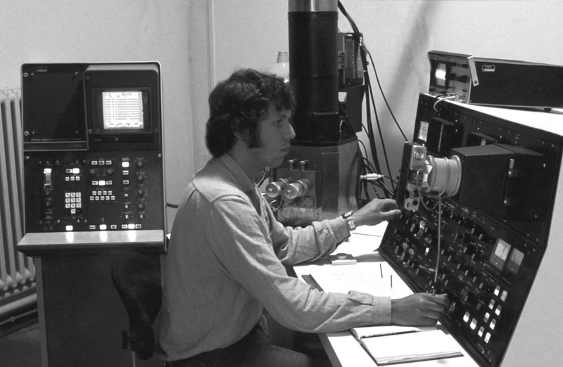
Image credit: [Hannes Grobe] CC-BY-SA 2.5


“SEMs don’t require sample preparation, but they really don’t”
Was that supposed to be “really do”?
Came to post this, from what I remember from SEM training was that samples should be made conductive by evaporating gold on them to prevent charging. Albeit high-pressure SEM and the likes do exist
Yes of course. If you read the rest of the sentence, it’s pretty clear. Unless what you have is naturally conductive you almost certainly want a gold coat. Insulators do poorly in a SEM.
I really like the looks of the 1948 philips EM-100. could be used as an 1950 scifi movie prop.
https://it.m.wikipedia.org/wiki/File:Electron_microscope_EM100,_Museum_Boerhaave_Leiden.jpg
Theremin cue. With this atomic beam weapon I rule the world…(booming reverb voice) no one can stop me now hah hah…
Our community college was able to get one, when they opened a new STEM building.
https://www.quora.com/Are-community-colleges-a-better-source-to-teach-information-technology-as-a-trade-than-colleges-and-universities/answer/Steve-Heckman-1
I also made use of one (indirectly) when I sent some PCB samples to a local lab to be analyzed. We were having a soldering issue, and foud that the RoHS solder had 3% lead (in other words, not RoHS)
Another Excellent topic by Asianometry! Well researched
Yeah applied science made a homemade semi in his garage.
https://youtu.be/VdjYVF4a6iU?si=ZWpGg2M8S0xjed3Y
Sem*
Even can hook up to an Arduino too
https://youtu.be/ruuxn2u3yao?si=WOz6qb5IzN_xX5ev
And today you can buy a desktop scanning tunneling microscope with atom-level resolution. Amazing.