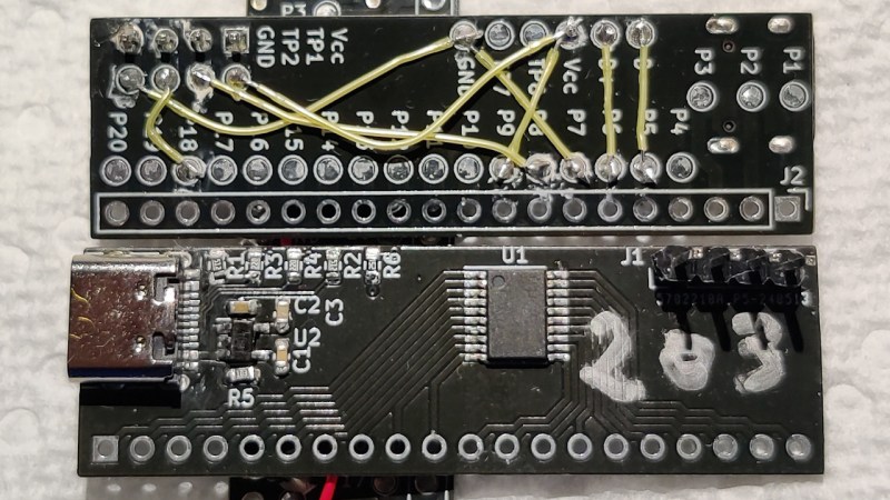
There are so many new cool MCUs coming out, and you want to play with all of them, but, initially, they tend to be accessible as bare chips. Devboards might be hard to get, not expose everything, or carry a premium price. [Willmore] has faced this problem with an assortment of new WCH-made MCUs, and brings us all a solution – a universal board for TSSOP20-packaged MCUs, breadboard-friendly and adaptable to any pinout with only a few jumpers on the underside.
The board brings you everything you might want from a typical MCU breakout – an onboard 3.3V regulator, USB series resistors, a 1.5K pullup, decoupling capacitors, and a USB-C port. All GPIOs are broken out, and there’s a separate header you can wire up for all your SWD/UART/USB/whatever needs – just use the “patch panel” on the bottom of the board and pick the test points you want to join. [Willmore] has used these boards for the CH32Vxxx family, and they could, no doubt, be used for more – solder your MCU on, go through the pin table in the datasheet, do a little point-to-point wiring, and you get a pretty functional development board.
Everything is open-source – order a few of these boards from your fab of choice, and you won’t ever worry about a breakout for a TSSOP20 MCU or anything that would fit the same footprint. It could even be used in a pinch for something like an I2C GPIO expander. This is also a technique worth keeping in mind – a step above the generic footprint breakouts. Looking for more universal breakouts to keep? Here’s one for generic LCD/OLED panel breakouts.


With 2L boards running $2/5 and this requiring SMT anyway, I’m normally just inclined to order purpose-designed boards than ever mess with jumpers.
yeah this board is for whenever you’re not feeling inclined to do that =D
Very much agreed and that’s what I did for the CH32V003–in three different packages. But, the shipping at JLCPCB is so cheap that I ended up getting 100 boards because it barely costs anything more (that’s the most I could get at 0.8mm thickness for the cheapest shipping). Now I have 90+ boards of various packages that I don’t have much hope of using.
Then I wanted to try the CH32V03X faimily and the CH32V203 chips which have completely different pin-outs than the 003. So, I would need to make even more custom boards. I started to think that ‘this might not be the best way’ to make dev-boards for just a few chips–if you’re making a dozen or a hundred, yes, make a custom board. But for one or two?
I could have easily modified my 003 design for the 033 and 203. That’s a day’s worth of tinkering around in KiCAD and staring at data sheets to make sure I got all the signals in the right place and didn’t forget something important (like a 1.5K pullup for USB signaling). Then there’s the two week wait for the boards to get back. That’s a fine way to go about it, but it occurred to me that I might have a better way for small batches of dev-boards and that’s what lead to this design.
Two issues have already been opened on the github for the project (thanks!) and both of them have the same kind of ambiguous answer. One asked for a stencil. Well, yes, I can generate one, but the reason I didn’t is because this is really meant to be use for small numbers of builds (at any one time at least) and hot air or hand soldering works just fine with the 0603 and TSSOP20 packages. I’ll generate a stencil file for those who want one since it’s pretty easy to do.
The other issue was asking for a BOM. That one is harder. Since each chip you build one of these up for will be different–there’s really no one true BOM. Does the chip need series USB resistors? Does it need a 1.5K pullup? What voltage does it run at? What’s the input voltage you want to feed the regulator? Are you even using USB-C? There are so many different ways you could build out the board, it doesn’t make sense to have a BOM. That said, I am going to add some BOM guidance to help people pick reasonable parts based on what they need. I just can’t give one that will fit everyone.
Hey did you ever think of putting a QFN20 under the tssop Package to allow for even more mcu types?
I don’t know if it fits under there. I could do a different board with just the QFN20 if there’s interest.
Really, this board ought to be designed as a set, with some for TSSOP (might as well go to 28, leave some pads connected if chip is only 20 pins), SOIC, QFP and horrid QFN (Rasp Pi, why didn’t you give the rp2040 actual leads?). Double points if you can overlap all those footprints without shorting.
Those footprints don’t play nice with each other. To fit all of those footprints on a board would require much more complex routing and we might end up with a 4 layer board. Now, those aren’t as expensive as they used to be, but I don’t know by how much.
I will point out you can already mount a QSOP28 on the TSSOP20 pads–they have the same lead to lead spacing, but slightly different distance between the rows of pins. You will have to decide which of the 4 pairs of pins on the ends you are willing to give up.
The reason not to make boards like this much larger than 20 pins is because they get unwieldy for use on breadboards–unplugging them starts to take a lot more effort. And you are limited to the size of breadboard they’ll work with. You quickly get into the area where a custom board makes a lot more sense.