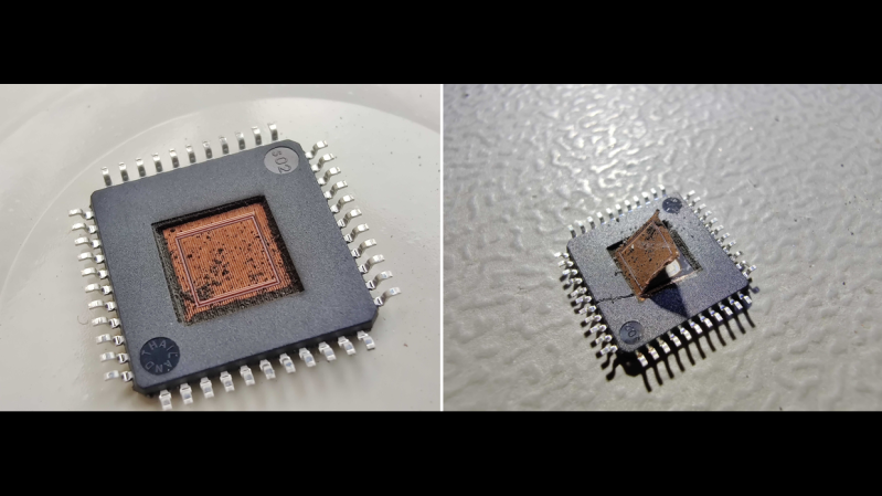
Whether the goal is reverse engineering, black hat exploitation, or just simple curiosity, getting inside the packages that protect integrated circuits has long been the Holy Grail of hacking. It isn’t easy, though; those inscrutable black epoxy blobs don’t give up their secrets easily, with most decapping methods being some combination of toxic and dangerous. Isn’t there something better than acid baths and spinning bits of tungsten carbide?
[Janne] over at Fraktal thinks so, and the answer he came up with is laser decapping. Specifically, this is an extension of the laser fault injection setup we recently covered, which uses a galvanometer-scanned IR laser to induce glitches in decapped microcontrollers to get past whatever security may be baked into the silicon. The current article continues that work and begins with a long and thorough review of various IC packaging technologies, including the important anatomical differences. There’s also a great review of the pros and cons of many decapping methods, covering everything from the chemical decomposition of epoxy resins to thermal methods. That’s followed by specific instructions on using the LFI rig to gradually ablate the epoxy and expose the die, which is then ready to reveal its secrets.
The benefit of leveraging the LFI rig for decapping is obvious — it’s an all-in-one tool for gaining access and executing fault injection. The usual caveats apply, of course, especially concerning safety; you’ll obviously want to avoid breathing the vaporized epoxy and remember that lasers and retinas don’t mix. But with due diligence, having a single low-cost tool to explore the innards of chips seems like a big win to us.


The article is well written, and I like the rest of the series as well. The short history lesson on packaging is quite thorough. The part on decapping is correct, but it wasn’t as clear to the approach. As where there are a dozen safe decapping methods, most are destructive and are useful for chip analysis under the microscope. Recently, Richi from Richi´s Lab introduced a small oven built from a power resistor to decap chips. But some people over at the Siliconpr0n Discord from John McMaster seem to have great results with a simple torch.
There aren’t many ways found to decap from the front side while keeping the chip a live, sadly. Fraktal shows laser decapping from the backside, which is a common method for attacking these chips. I’m surprised they can decap in a reasonable time with just a 2W laser, as usually much more powerful lasers are used.
Chip preparation for laser FI is usually quite expensive, as you don’t just want access to the backside of the chip, you want the chip as thin as possible. A thinner die attenuates the laser pulse less. Thinning a chip to sub 50 um is not an easy task, but it could be done with a Dremel in a CNC and loads of time. Lastly, you want to have the best surface finish on the die, for the best FI success. I’m expecting the thickness and polish will have large effects on the relatively low power lasers Fraktal uses.
I hope Fraktal will continue the series, as I like to see the FI results they have achieved. For the home player, I’d look at BBI, instead. As it can achieve similar effects, but is more accessible to the hobbyist.
Here are the threads from Richi with details about their methods including the oven. https://www.eevblog.com/forum/projects/decapping-and-chip-documentation-howto/
Aww man, what an excellent way to continue die exploitation series. Excellent work!