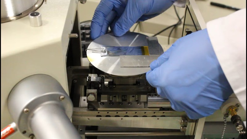
If you want to build semiconductors at home, it seems like the best place to start might be to find a used scanning electron microscope on eBay. At least that’s how [Peter Bosch] kicked off his electron beam lithography project, and we have to say the results are pretty impressive.
Now, most of the DIY semiconductor efforts we’ve seen start with photolithography, where a pattern is optically projected onto a substrate coated with a photopolymer resist layer so that features can be etched into the surface using various chemical treatments. [Peter]’s method is similar, but with important differences. First, for a resist he chose poly-methyl methacrylate (PMMA), also known as acrylic, dissolved in anisole, an organic substance commonly used in the fragrance industry. The resist solution was spin-coated into a test substrate of aluminized Mylar before going into the chamber of the SEM.
As for the microscope itself, that required a few special modifications of its own. Rather than rastering the beam across his sample and using a pattern mask, [Peter] wanted to draw the pattern onto the resist-covered substrate directly. This required an external deflection modification to the SEM, which we’d love to hear more about. Also, the SEM didn’t support beam blanking, meaning the electron beam would be turned on even while moving across areas that weren’t to be exposed. To get around this, [Peter] slowed down the beam’s movements while exposing areas in the pattern, and sped it up while transitioning to the next feature. It’s a pretty clever hack, and after development and etching with a cocktail of acids, the results were pretty spectacular. Check it out in the video below.
It’s pretty clear that this is all preliminary work, and that there’s much more to come before [Peter] starts etching silicon. He says he’s currently working on a thermal evaporator to deposit thin films, which we’re keen to see. We’ve seen a few sputtering rigs for thin film deposition before, but there are chemical ways to do it, too.


Back in the 80s, electron-beam microlithography was the way all semiconductor production masks were made, since 1:1 projection aligners were in use at the time. Then reduction steppers came into use, and we went back to optically printed reticles. Not sure what they use now.
Anyway, I worked for a company that used direct-write lithography for customising gate arrrays. We built our own machines, which were glorified SEMs, but with beam blanking, pattern generator, stepper motor driven x-y stages, airlock, a deflection system with low distortion at high deflection .. and crucially, methods to align with features on the substrate.
We worked with gate arrays, since that meant that everything except the final metallisation pattern had already been fabricated. Otherwise the range of equipment you need is overwhelming.
Making your own transistors is going to be impossible, I think. I did manage it as a post-grad using spin on dopants and optical masks, but without ion-implantation you will never be able to achieve very small scales. – my transistors were millimetres in size and pretty low performance.
Still, I guess it’s about the journey and not the destination, so have fun!
“Making your own transistors is going to be impossible, I think.”
See Sam Zeloof YouTube channel link below.
implant isn’t used for GAA transistors, it’s all epitaxial
Every step we take closer to maker micro-fabs is exciting. Hopefully in a short time it’ll be as cheap and easy to have a custom chip made as it has become to have something 3D printed.
This is so cool I don’t even know where to start. But I do wonder how people have time to do stuff like this. I have about a million projects I’d love to tackle but making HaD comments for 10 minutes with morning coffee is about all I can muster. I guess single with a 9-5 job? Anyway, I’m happy (and jealous) of projects like this. Very cool.
Reminiscent of my second job, in 1968-75, at the Westinghouse R&D Center. We had the old prototype SEM, built by Oliver Wells, modified to draw rectangles stored as seqential points on mag tape by a Burroughs mainframe from a card deck. The resist was PMM. We knew it would always be too slow, so the goal was to make a metal mask. That mask was put in a vacuum and magnetic field, hit with UV, and the emitted image was 1:1 projected onto a PMM-coated wafer. When I left, our best linewidth was just under a micron.
Good luck with your project.
I did this once on Apple 2 computer with 12 bit D/A card and a 1968 Cambridge StereoScan SEM for work.
We needed to test eBeam resists. The SEM was mostly vacuum tubes with only a few of the modules being transistorized. 12 bits provided 0.25µm resolution and a 1mm^2 pattern area. The vector code was in 6502 assembly and could write points, lines, rectangles and alphanumeric text with a 5×7 dot matrix font copied from a Macintosh computer (Courier I think). Good times…
Another guy making homebrew ICs:
https://www.youtube.com/@SamZeloof/videos