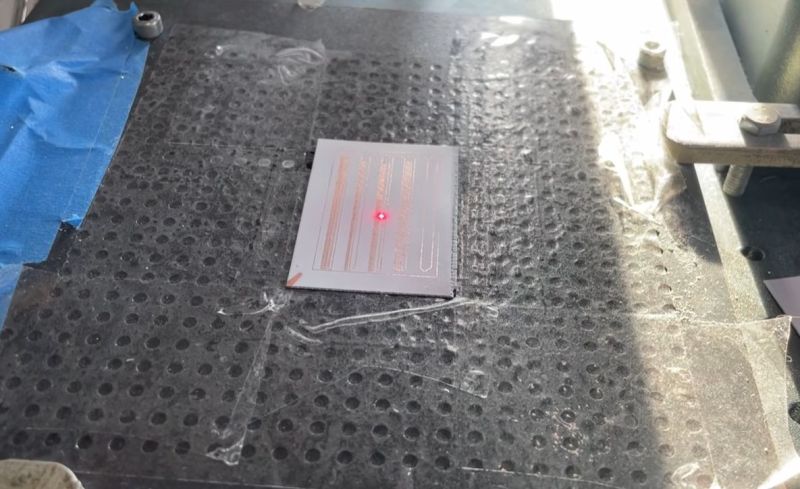
Creating PCBs at home is quite easy these days (vias not withstanding), but even the best DIY methods usually can’t match the resolution offered by commercial PCB production lines. Large traces are easy enough to carve out of copper-backed FR1 or FR4 with even a mill, what if you need something more like 100 µm sized traces with similar clearance? This is what [Giangix] has been experimenting with, using both a fiber laser and chemical etching to see what approach gives the best results.

The thin copper clad boards are put on the 20 Watt fiber laser and held in place with the vacuum table that [Giangix] previously made, using the power of suction to make sure the board doesn’t move. The used laser specifies a minimum line width of 0.01 mm, so that’s clearly fine enough to engrave away the chemical resist layer that is sprayed on top of the copper layer.
After some experimentation, it was found that increasing the trace clearance between the 0.1 mm traces to a hair above 0.1 mm was necessary for the subsequent chemical etching step to work the best, as otherwise some copper was still likely to remain. The chemical etching bath mixture consists of hydrochloric acid and hydrogen peroxide, in a ratio of 2 mL water to 2 mL 30% HCl and 2 drops of 35% H2O2. This is agitated for 90 s to get a pretty good result.
Although the final resistance measurements on the traces is a bit higher than theoretical, comments suggest that maybe some of the copper got removed along with the removal of the resist layer. Perhaps the most interesting question here is whether directly ablating the copper using the fiber laser would give even better results and bypass the etching chemicals.


Etching boards at home with laser printer, photo paper and ferric chloride was fun 15 years ago when no other option was
availableviable to make your own sumo robot with real PCB and real surface mount parts. Nowdays I’d rather order from China and just wait 3 weeks instead of wrestling with chemicals and then dealing with board that has no solder mask.+1
Depends on how fast you want to iterate. If you want to test something the same day, it’s hard to avoid making your own pcbs.
I used to do the same when I was making BBQ and smoker controllers. I have been using a service from Portland, OR. called OSHPark. Not sure where they get the board made persay, but it usually took about a week to get the boards. You get 3 copies at a time. Been using them for close to 15 years, I believe.
OSHPark’s boards come from a variety of domestic (US) board houses, depending on when the panel goes out and (I assume) manufacturer’s availability.
Clearly you are a much more patient person than many of us
If it was fun 15 years ago it aught to still be fun now…
But really it is hard to argue with quick cycle times of doing it yourself, and it is nice to know your designs are still your own for many. Also you can also add a solder mask if you like, its another step but you are still talking a handful of minute to get that double/single sided board, and being able to debug quickly even when your mistake turns out to be nearly impossible to bodge wire – something I’d suggest is getting more common as SMD parts trend smaller and PCB traces must get denser around them.
You can apply solder mask yourself and then just scrape it away on the pads you need to access.
Stephen Hawes has some great videos and resources for this. I’ve also been experimenting with this, but I cheaped out and got a 5W fiber laser. I’ve had no good results so far.
I was experimenting with lasering PCB traces last week on a 50 W fiber laser at work and the real problem is getting through the copper evenly without blasting through the FR4. Didn’t watch the video but I’m guessing that’s one reason for the chemical etch.
I get the argument against making your own boards since you can get 5 boards in 3 weeks for literally $5 from JLC, but… I also want to make my own boards. So I did. Ended up milling instead since I know it works but I dialed the laser in on some shim stock and got a nice stencil for the mcu on that $5 board I’m still waiting for hah
Safe disposal of copper salts seems more feasible than the safe treatment of air contaminated with metal vapours.
I had applied to the Hackaday Superconference last year for a talk on ablation using fiber laser to make PCBs but had to pull out from travelling and presenting it at the very last moment.
The issue with fiber lasers, as others have rightly pointed out is that it’s difficult to control the process at the boundary when you run out of copper and ablate FR4, it generates heat and smoke and causes blackening which compromises the integrity of the fiberglass. It needs time to tune the parameters to get results (frequency, power, pulse duration) and I got close but not fully there where I expected it to be – and that’s what I would have presented. And I think that’s why people opt for the simpler route to just do ‘lithography with laser’ and do chemical etching post that.
It’s very precise and will get good results. You can even use gantry laser cutters/CO2 laser cutters for this which could be cheaper than a galvanometer based solution.
I do plan to work on the copper ablation approach further, let’s see.
Good luck man, we’d all be rooting for you.
Fibre laser may not be the best one for making PCB by ablating copper 355 nm UV laser is a better option as copper absorbs it better and with a short pulse its possible to get clean cut without charring FR4 material. The laser power needs to be less than 5W. In the past I have used tool by LPKF that uses this approach however the version of the tool we had a pathetic UI software that would fail in the middle more over the laser had some nonlinear optics which need 24×7 air-conditioning as they were sensitive to humidity which meant the beam lost its focus very often.
I’ve been exploring the idea of etching PCBs with my 12W UV laser, then using a fiber laser to drill & char throughholes, with the goal of copper plating over the conductive char. Gemini says this should work (and even provided laser setting recommendations), for whatever that might be worth.