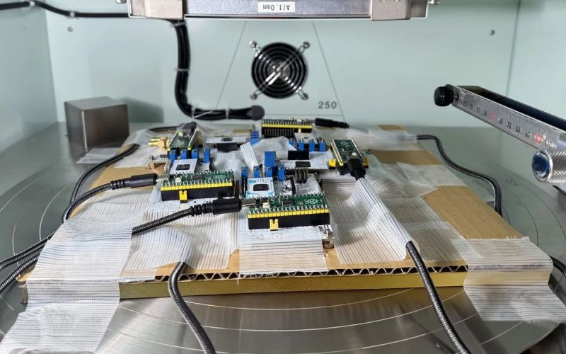
Ionizing radiation damage from electrons, protons and gamma rays will over time damage a CMOS circuit, through e.g. degrading the oxide layer and damaging the lattice structure. For a space-based camera that’s inside a probe orbiting a planet like Jupiter it’s thus a bit of a bummer if this will massively shorted useful observation time before the sensor has been fully degraded. A potential workaround here is by using thermal energy to anneal the damaged part of a CMOS imager.
The first step is to detect damaged pixels by performing a read-out while the sensor is not exposed to light. If a pixel still carries significant current it’s marked as damaged and a high current is passed through it to significantly raise its temperature. For the digital logic part of the circuit a similar approach is used, where the detection of logic errors is cause for a high voltage pulse that should also result in annealing of any damage.
During testing the chip was exposed to the same level of radiation to what it would experience during thirty days in orbit around Jupiter, which rendered the sensor basically unusable with a massive increase in leakage current. After four rounds of annealing the image was almost restored to full health, showing that it is a viable approach.
Naturally, this self-healing method is only intended as another line of defense against ionizing radiation, with radiation shielding and radiation-resistant semiconductor technologies serving as the primary defenses.


.. why not just use EMP-safe tube technology instead?
An Vidicon or Orthicon camera with filters for different wave lenght can do it, too.
I have trouble understanding why a fragile trash technology such as CMOS has to be shoehorned into such an application if there’s a more elegant solution available for decades.
Poor sensitivity and resolution, fragile design, susceptible for magnetic interference, high power consumption.
Thanks, I think these are valid points.
I just wonder if a more modern version of the video tube could improve things.
Or maybe a variant of CCD technology.
If Starship ever works, you could have a mix of technologies.
Late 1970’s tech is a sweet spot, not too primitive, not too complicated.
Voyager Probes, had they been built earlier or later, may not have lasted as long.
I wish the microchip had been invented much later…on a Moonbase, so as to keep launch vehicles massive.
This user is a performance art piece, right? Like an Onion bit about “Area Man Reflexively Hates Everything Invented After 1963, Insists on Telling Internet” but stretched out across years?
I view it as compulsive infodumping that veers into personal preference signalling. However on a few occasions I have found his insights were on topic and interesting.
Nah, I’ve always recognized the positive aspects of tube technology, while others loved to criticise it or make fun of it for a cheap laugh.
It’s otherway round, thus, I think. The US is historically unrationally being obsessed with anything solid-state technology.
And finds complex solutions for problems that wouldn’t exist in first place if another, simpler technology was used to begin with.
Way back in the mid-20th century, development of tube technology had been basically stopped because of this unhealthy obsession.
Nuvistors proved that tube technology wasn’t a dead end yet.
They were being used in satellites, too, exactly because of being robust against radiation.
Also, I was raised to not to criticise people on a personal level.
Doing so often is a sign that someone runs out of good arguments. :)
Even the vacuum technology will encounter the same problems with radiation/flying particles sensitivity when it will be miniaturized near atomic scale. Change my mind:)
Agree on your point of not dropping the discussion down to the level of personal attacks. It should be all about mutual learning here, not snarkiness…
The basic problem is that compared to doped silicon, vacuum doesn’t conduct very well. A flake of silicon almost not visible to the naked eye can control tens of milliamps with a supply of 2 volts and an inherent capacitance of femtoFarads. A tube with a supply of 50 volts can’t be as small as a cubic millimeter and control one milliamp, and will still have over a picoFarad grid-cathode capacitance. That makes tubes slow and power hungry in most applications.
Specialized radio frequency applications can have traveling wave tubes, klystrons and magnetrons. Their construction is labor intensive. Fast complex circuitry excludes tubes.
Tube manufacturers didn’t give up. For instance, there was am attempt to build an addressable low voltage flat vacuum video display. It couldn’t be made practical.
“Nature abhors a vacuum.” So do pets and modern electronics.
Found some interesting examples from a quick Google search…
8K HARP Tubes (NHK/Hitachi): These experimental tubes were capable of resolving up to 2,000 TV lines. Developed by NHK’s Science & Technology Research Laboratories, they used avalanche multiplication in an amorphous selenium target to achieve ultra-high sensitivity and resolution required for the initial 8K Super Hi-Vision prototypes.
Return Beam Vidicon (RBV): Used in specialized scientific applications like the Landsat satellites, these tubes could resolve approximately 6,000 lines. They functioned similarly to a 3-inch Image Orthicon but were primarily used for high-detail monochrome earth imaging rather than standard video production.
Hi-Vision (Analog HDTV) Tubes: Standard 1-inch Saticon or Plumbicon tubes used in Japan’s “Hi-Vision” analog HD system (developed in the 1970s and 80s) provided roughly 1,035 to 1,125 lines
I had a feeling that the origin this led back to the amazing hacks on the Junocam. Sure enough the IEEE Spectrum article calls it out in the 3rd paragraph.
I will link to my comment from a few months ago!
https://hackaday.com/2025/07/23/annealing-in-space-how-nasa-saved-junocam-in-orbit-around-jupiter/#comment-8153111
Innovating is just hack, refine, and repeat, no matter where you work.
The SOHO/EIT sensor has been getting regularly baked throughout its entire mission, just out of commission for weeks at a time. The linked article describes some of the other purposes the bakeout serves.
https://www.esa.int/Science_Exploration/Space_Science/What_is_a_SOHO_EIT_CCD_bakeout
Vacuum tube technology is not more elegant than CCDs or CMOS imagers. Quixotic and Quaint are likely better adjectives. It’s abandoned technology, frozen in time, and as such its low resolution, low frame rate, reduced dynamic range, and raw inexperience in rocket-launched platforms operating outside of low earth orbit make it a bad risk.
Or, what OH3MVV said.
Because Arizona was not a high radiation environment back when they were faking the moon landings…