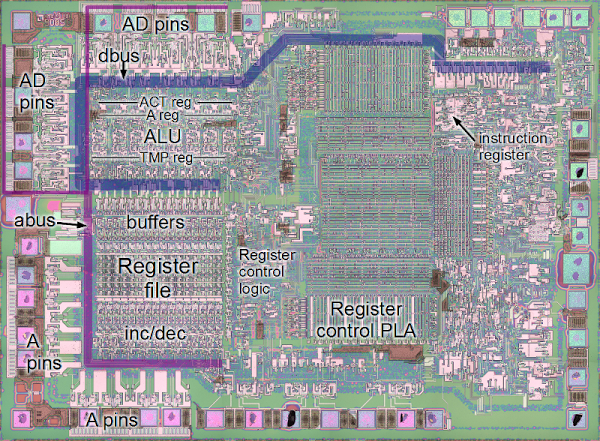
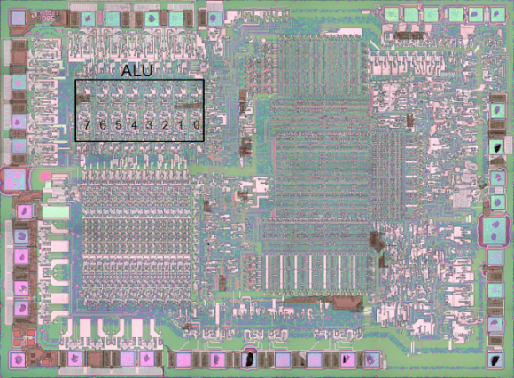
Hardware design enthusiasts should already be salivating just looking at this image. But [Ken Shirriff’s] write-up on how the 8085 processor’s registers were designed will put you in silicon reverse-engineering heaven. He manages to get to the bottom of the tricks the designers used to make register access as efficient as possible, like routing some through the ALU on their path elsewhere.
We’re certainly not experts in studying dies like the one seen above. Luckily [Ken] does a great job of zooming in on important parts, then dissecting how they work by representing the silicone image as a functional flow chart. One of the parts which we found most interesting is the WZ temporary registers. These are a set of internal registers that are not accessible to the programmer. They’re only used internally by the chip. They act as temporary storage for multiple operand functions, and also hold register addresses for a handful of instructions (JMP, CALL, RST, etc.).
If you’re more interested in how images of these chips are attained you should do some searching on Hackaday. Just last week we featured one such project in a links post.
[via Reddit]


