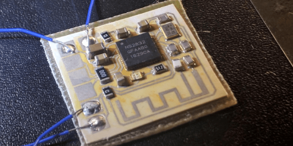
In a previous episode of Hackaday, [Rich Olson] came up with a new no-etch circuit board fabrication method. And now, he’s put it to the test: building an nRF52 Bluetooth reference design, complete with video, embedded below.
The quick overview of [Rich]’s method: print out the circuit with a laser printer, bake a silver-containing glue onto the surface, repeat a few times to get thick traces, glue the paper to a substrate, and use low-temperature solder to put parts together. A potential drawback is the non-negligible resistance for the traces, but a lot of the time that doesn’t matter and the nRF52 reference design proves it.
The one problem here may be the trace antenna. [Rich] reports that it sends out a weaker-than-expected signal. Any RF design folks want to speculate wildly about the cause?
Continue reading “No-Etch: The Proof In The Bluetooth Pudding”


