Testing The Limits Of Home PCB Etching

[Quinn Dunki]’s Veronica, a homebrew computer based on the 6502 CPU, is coming along quite nicely. She’s just finished the input board that gives Veronica inputs for a keyboard and two old Nintendo gamepads. [Quinn] is building this computer all by her lonesome, including etching all the PCBs. She’s gotten very, very good at etching her own boards, but this input board did inspire a few facepalming moments.

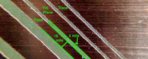
In an earlier post, [Quinn] went over her PCB etching capabilities. As demonstrated by the pic above, she’s able to print 16 mil traces with 5 mil separation. This is just about as good as you can get with homebrew PCBs, but it’s not without its problems.

[Quinn] is using a photographic process for her boards where two copies of a mask is printed on an acetate sheet, doubled up, and laid down on a pre-sensitized copper board. The requirement for two layers of toner was found by experience – with only one layer of toner blocking UV light, [Quinn] got some terrible pitting on her traces and ground planes.

Two photographic masks means the masks must be precisely aligned. This example shows what happens when the acetate sheets are ever so slightly misaligned. With a 5 mil gap between traces, [Quinn] needs to align the masks to within ±2.5 mils; difficult to do by eye, and very hard once you factor in flexing and clamping them down to the copper board.

Even when this process goes perfectly, [Quinn] is pushing the limits of a laser printer. When printing at 600 dpi, the pixels of the print are about 1.5 mils. While GIMP, printer drivers, and the printer itself have some fancy software to help with the interpolation, [Quinn] is still seeing ‘bumps’ on the edges of perfectly aligned parts. This is one of those things that really makes you step back and realize how amazing fabbing PCBs at home actually is.

With most of the hardware for Veronica out of the way, it’s just about time for [Quinn] to start programming her baby. We’re not expecting a full-blown operating system and compiler, but those NES gamepads are probably crying out for some use.

10 Ways To Etch PCBs At Home

[youtube=http://www.youtube.com/watch?v=Q4tWEse2rDI&w=580]

There are a ton of benefits for etching your own circuit boards at home, chief among them the ability to design a circuit in the morning and have a prototype in your hand by lunch. There’s always the question of how to etch the board, but [NurdRage] over on Youtube has all the chemistry covered on ten different etchant solutions for DIY PCB manufacturing.

The peroxide-based methods use simple over-the-counter Hydrogen Peroxide to remove all the copper on a PCB. By combining H2O2 with either Hydrochloric (muriatic) acid or Sulfuric acid, you’ll get a relatively easy to acquire and somewhat safe etching solution.

Historically, the favorite etchant for the home PCB manufacturer has been Ferric Chloride and is still surprisingly available at a few Radio Shacks around the US. Another chloride etchant – Copper Chloride – is one of the most reusable etchants available, able to be regenerated by simply bubbling air through the solution. You can actually make Copper Chloride etchant by reducing down the products of an H2O2 + HCl etchant, making this a very good etchant for PCB pros.

In the ‘miscellaneous’ category, [NurdRage] goes over some alternative etchants such as Bleach and HCl, Nitric acid, and potassium nitrate and HCl; the potassium nitrate etchant is fairly similar to aqua regia, so if you’ve ever wanted a gold PCB, this is the way to go.

Balancing the ease of production and safety of all these etchants, we’ll stick with our Hydrogen Peroxide and HCl etchant for now, at least until we move up to CuCl for the best etching machine we’ve ever seen.

Continue reading “10 Ways To Etch PCBs At Home”

Etching Your Own PCBs At Home

Etching your own PCBs from copper clad board is nothing new, but the ability to make your own circuit boards at home is so useful it should be part of every maker’s repertoire of skills. The folks over at Hub City Labs in Moncton, NB, Canada put together a workshop covering the basics of home PCB manufacturing, allowing any maker to put a circuit board in their hands in under an hour.

The process starts just like any PCB design – laying out traces, parts, and vias in a PCB designer such as Eagle. When making your own boards, it’s a good idea to make the traces and pads extra large; the folks at Hub City Labs follow the 50-50 rule: 50 mil wide traces with 50 mils of seperation.

The PCB design is printed out with a laser printer (in mirror mode) onto a piece of paper from a glossy magazine or inkjet photo paper. After the copper board is scrubbed to remove any oxidation or oils present, the design is laid face down on the copper and heated with a clothes iron or sent through a laminator.

After the laser printer toner is transferred to the copper, the recipe calls for etching the board with a solution consisting of a half cup of 3% Hydrogen Peroxide and a quarter cup of muriatic acid.

The folks at Hub City Labs put together a great tutorial for one of the most useful skills the home electronics wizard can have, but etching your own PCBs is an art unto itself. There’s a lot of ways this process can be improved, from using Kapton tape to secure the printed art to the copper board, to getting high-strength peroxide from a beauty supply store.

If you’ve got any tips on making your own PCBs at home, drop a line in the comments below.

EDIT: Good job killing Hub City Lab’s web server, everybody. They’re working on getting something up.