It’s never been easier to get a printed circuit board made. In fact, almost every electronics video out on the internet will incessantly remind you of this fact now. But making a custom PCB wasn’t always as straightforward as sending a KiCad file to a board house. Many DIY methods involve harsh chemicals and tedious processes, but did have the potential benefit of taking much less time than waiting on boards to arrive in the mail. [Bettina Neumryr] is demonstrating one of these older methods, called the toner transfer method, using a circuit that was printed directly in an old magazine.
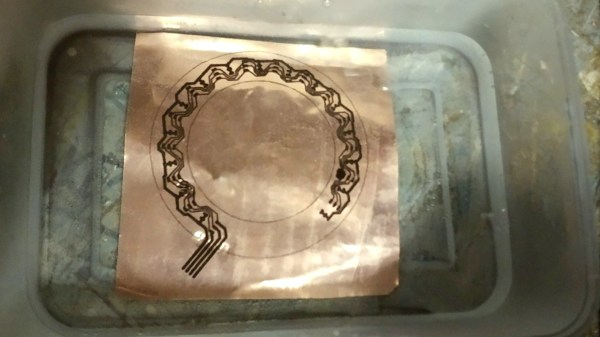
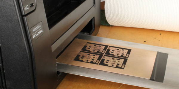
The first part of the toner transfer method is to create an image that can be printed. Since this circuit came from a magazine, it is first scanned in to a computer and imported into GIMP, where it can be scaled to match the size of the components and then sharpened to make a crisp print. With the image ready, it’s time to print the image onto some toner transfer paper, ensuring that the printer in question is a laser printer which actually uses toner. From there, a sheet of blank copper PCB is prepared and then the toner is transferred by heating, in this case using a laminator. After that its etched, removing all of the copper not protected by the toner, and then the toner itself can be removed which leaves behind the copper traces.
For those of you who were around when toner transfer was in vogue, this video might not have much value. But for anyone who can’t use a board manufacturer for whatever reason or is looking for alternatives, a modern video showing the method could be much more useful and have better context for beginners than videos made a decade or more ago now. Some of those older methods include similar processes using inkjet printers instead, but there are more modern DIY methods as well using lasers or CNC machines too.