If you’ve ever made double-sided PCBs without professional equipment, you had to deal with connecting one side of the board to the other. You have a few obvious choices: 1) Rely on component leads to connect both sides (and solder both sides); 2) Create vias and solder wire to both sides of the board; or 3) Use through hole rivets. [Diyouware] had a different idea: use conductive ink. After a few false starts, they found a technique that seemed to work well.
This isn’t the first time we’ve heard of people trying conductive ink with varying degrees of success. The biggest problem, usually, is that the ink wants to run out of the hole. [Diyouware] has an interesting solution for this problem: Don’t drill the hole all the way thorough.
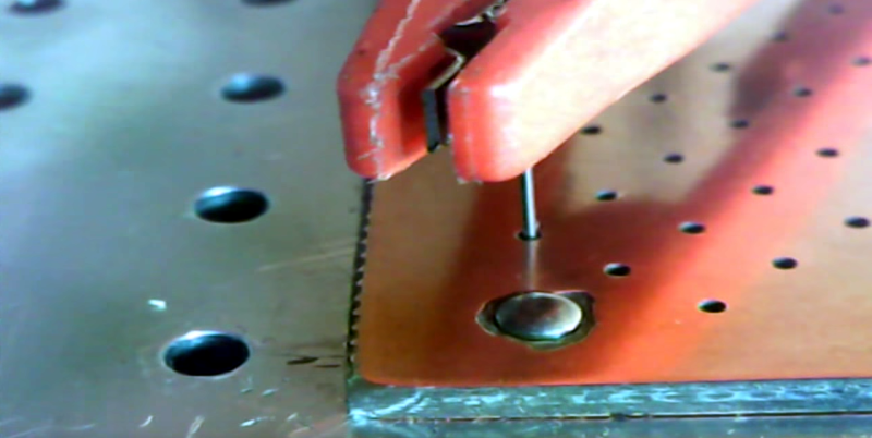
To do this reliably, [Diyouware] modified a drill press to get a signal when the bit makes contact with the bottom layer of copper. The result is a blind via that forms a well. It is a simple matter to fill that well with conductive ink later. Although you could fill the vias by hand, [Diyouware] used a dispenser robot and controlled it with output from an Eagle user program to convert the via pattern into machine instructions. You can see the creation of an experimental board in the video below.
It is worth noting that when you have a PCB made professionally, they often drill a blank board and then plate it, so the pins and vias conduct through with no difficulties. In addition to the plating, this also makes it challenging to get the artwork exactly lined up with the holes. There are other professional processes, too, that plate boards after drilling and the plating part is possible.
LPKF has a method for faking plated through vias, that also uses a conductive paste. Of course, one easy way to get nice plated through vias (and holes) is to just go ahead and have the boards made professionally.


Problem is:
1. How do you get the conductive ink to contact the TOP side copper, the side with the hole, reliably.
2. Conductive ink really isn’t very conductive. It’s one thing to use conductive ink as an activator for electroplating, but using it to actually carry the electrons in use for any appreciable current or longevity I suspect not.
+1.
And I would add: how is that “contact point” between the ink and the copper going to react when the board will be heated up for soldering?
Hi Pinhead,
Most of the nano-particles inks requires and annealing process at 100-240ºC depending on the ink formulation. So the ink will cure at the same time you solder the board on the reflow oven, although you can use a simple hairdryer to cure it because the amount of ink injected in each via is so small that it cure very fast.
Hi James,
Answering your first question: the ink formulation includes an adhesive with adhere to the well walls and the top layer. Second question: the ink we are using is a copper nano-particles ink we brewed at home. It’s easy and safe making it at home, but the method is not very productive and copper oxidizes quickly. You can use a better ink (not paste) made with silver nano-particles. It’s more expensive but has an excellent conductivity. There was recent researching about this kind of inks with very good results.See http://pubs.acs.org/doi/abs/10.1021/ja209267c Even you can brew it at home: see this video: https://www.youtube.com/watch?v=EBlqPS8boLI based on the paper. Vias are really very small 1.6mmX0.8mm in our testing; I mean they are not long ink traces where you probably could have resistivity issues.
There something I don’t understand in this video. We don’t see the ink coming out of the hole! Consediring the needle is almost as large as the hole even thought it would come flush when the needle retreat the ink will flow down so the top layer would not contact with the top layer.
Hi Jacques,
Please, read the blog. We explained there everything.
The project is not closed and the video is only a proof of concept. When we saw it was feasible we wanted to share immediately the idea and we published the video, but we are still testing and brewing ink. We explain all in the blog article and we will publish the complete results in the following weeks.
Thanks.
For better contact the top hole could be tapered
Back in the day I milled PCBs. I setup the routing to take advantage of the leads when it could. I setup isolation zones under the chips so there wouldn’t be any vias there. I setup the vias on another layer in the software. I would drill them into an overhead sheet using a backer board. I would use a larger drill bit so there was adhesion to the pad. I would squeegee the conductive epoxy on the top and bottom, pushing it into the holes. Then let it dry. Then dry it in the convection oven at a low temp. Then heat cure it. The problem was that the epoxy was not as conductive as wire. I used a custom mix from Poland. After the number of vias got up too high (50-100) I would get failed vias and it wasn’t as effective.
I’ve done much the same. I used a piece of paper towel behind the pcb to pull the ink into the hole. Usually had to do a little cleanup with acetone after the via had mostly dried. But I found it to work very well with small prototype boards.
A better way, conductively speaking, would probably be to fill the wells a bit more than flush with solder.
Hi dsblackout,
We tried, but when we heated the solder paste first it boiled spilling over the well and then it reduced its volume so much that it just rested on the bottom of the well. We also tried filling the well with copper dust, tin dust, or any conductive dust. It was impossible to get it into. Even dispense paste into the well could be difficult. For paste dispensing will be better through-hole vias because the air can escape through the other hole side. Our method works fine because the conductive ink is liquid and we can inject it into the well.
Instead of solder paste, how about coating the hole in liquid flux then filling with plain solder? The flux component of the paste wouldn’t be doing any good beyond the surface.
A lot of effort for a questionable result.
I’d stop at the drill stage and do what Dsblackout said… fill the holes with solder as needed when soldering the parts on the board and move on with life.
Actually for as coarse a hole as that is (even though it’s small) get a piece of copper wire nearly the same diameter and a few thousands longer and peen it into place, then solder. home made rivet
.
I was just thinking this, fill it with solder and move on :)
Of course! Why bother tinkering with conductive ink when simple and common solder does the trick?
Maybe, when you reheat the board the ink stays dry but the solder reflows?
isnt it already in a hole? where would it flow?
Yes, you are right. See my comments above.
My guess is that surface tension will prevent the solder from adhering to both layers trough such a narrow channel. Regarding the original idea, having made lots and lots of PCBs at home I’ve grown to find it too limiting to pursue anymore. We are all aware that the IC packages slowly go smaller and smaller. Most sweet chips on the market aren’t that friendly when you cannot reliably do <10mils. Many come with an exposed pad underneath, which should be heatsinked with an array of vias. High-frequency SMPS converters benefit from compact two-layer layout wit lots of vias. Soldermask prevents solder on grounded pins from flowing beyond the pad area.
I want to learn PCB design the real way, beyond the 12-mil traces, last-minute CD-marker fixes and tedious to make vias. That's why eventually i ditched homebrewing them entirely – in the days of dirtyPCBs, Shenzhen2U, Elecrow and others it seems just the only choice. There's only so far homebrewing PCBs will take you.
Only problem: surface tension of solder and flux don’t allow this. Every tried soldering from one side of the board to the other side at the edge? Only works with really large solder blobs.
You can’t just fill the holes with solder. That doesn’t work. Solder’s got too much surface tension to go down a tiny via. And solder paste wouldn’t work either: it’s not ‘liquid solder’, it’s solder mixed in with flux. So the flux would boil, and you’d never get enough solder to fill the hole. A large enough hole might be doable, but that’s not practical.
Thin copper wire is doable, but it’s very hard to form a flush via that way (which means vias under packages can be dangerous).
heat from the bottom to avoid surface tension problems.
Nice work! Always good to see people working on actually advancing what can be done with this kind of tech in a way that isn’t yet another firmware, electronics or bot variant.
Hi Myndale,
Thanks!
We think there are a lot of improvements in the process of making PCBs at home. Now that we can have 3D printers and affordable similar robots, we can questioning the traditional methods and try to find alternatives. This is what we are trying to do: a robot which help us to make PCBs prototypes at home.
How about just making two single sided pcbs and glueing them together after drilling the holes? This kind of pcb sandwich can also do 4 layers or more. I confess that I never tried it… but maybe I should ;)
It’s nice that they try to find some more advanced diy-pcb processes, but you should have to keep an eye out on the viability and trade offs of the diy fabrication and evaluate if there really is a problem to solve in the first place…
If the number of vias is small, soldering a piece of wire or using rivets is still A LOT easyer, cheaper and faster than using a specialized drill-rig, paste dispenser and very expensive conductive ink. If the number of vias is larger, i can not really depend on a diy-process that is not 99.9999% reliable. Trying to troubleshoot a complex circuit that does strange things because of a “semi-bad” via is not really my thing. If i order an electroplated board from a fab, at least i can request them to do flying probe tests on every via, so i know what i get. Every board with more than 2 layers is getting electrical tested anyway in every quality fab shop.
Hi Andreas,
In recent years, most of electronic hobbyists have been integrating more and more components in small, double-side SMD boards which have more and more vias. There is no alternative way to use vias (until somebody will invent 3D electronics and we will be able to print the circuits). We have some prototypes with 100 vias and it’s really time consuming and boring to solder them. Really I prefer that a robot do this hard work for me. This is what we are trying to do.
On the other hand: we are not trying to replace the fab boards. Now they have an affordable price and you can order 10Pcs x 14$ + shipping from China. But they take some weeks to arrive home. Also complex circuits using SMD components are difficult to test on breadboards. Frequently we make a first prototype using a real PCB and the try-error method with the fab could be expensive and frustrating.
We have a different vision. We think electronics designing has to be more interactive, similar to software development. Nowadays, we have powerful CAD programs, simulation software and we can order cheap boards to a fab, but there is a gap between the simulation software and the fab: the first prototype. Here is where we think we can use a robot to help us.
Thanks.
Hey Victor, thanks for your reply. You just brought up a very interesting point in your answer without probably realizing it.
In professional electronics design, we are actually using more and more software to simulate not only the schematic circuit, but at the same time use PCB simulations (signal integrity, power distribution, decoupling networks, EMI/RF-Sim…) and then go into the CFD domain to do the thermal simulations to actually validate a design BEFORE we even think about ordering real components and slap them on a pcb. The problem is that to validate a design in the virtual domain takes a lot of experience and know-how, and the tools are extremely expensive. I guess this is something that will not change in the near future.
You can just not compare hardware development with software, one is totally virtual and can very easily be built and tested in a virtual world before you let it run on a dedicated hardware, the other is depending on real world physics that we can not fully represent in a virtual world because of the complexity of the system and the lack of real world data to acurately represent all the involved physics without needing supercomputers to get a good enough result in our lifetime.
My perfect vision would be that we would not ever have to waste any components and boards for prototyping. Your vision sounds to me like you want to make as many iterations as you can, maximizing waste and pollution, just because you can. We should encourage designers not to be lazy and slap some components together to see what happens, but instead to simulate, calculate and plan your designs before you transform them in the physical world. (Right the first time is the goal!)
Shipping only cost $20 using DHL and takes 3 days. PCB fab is about 5 days,so China is pretty competitive to the non-rush proto place.
Since you are automating filling the via, may be the next step is to automate probing the via resistance after the fill.
Hi,
We already thought it! Did you read it in our blog?
Next step will be to automate probing the vias resistance, but even more.
Our bot now automates: drawing double-sided PCB with a laser, drilling holes, vias and blind-vias, dispensing solder paste and conductive ink, plotting, 3D printing, etc.
Next step will be probing vias, circuits, painting them using conductive ink, soldering, 3D printing electronics, even make silicon chips why not, mayonnaise, pop-corns, wafers or whatever, because we are in the silicon age, not the “copper” age. :-)
HaD seems to switch between articles about how you should NEVER make your own custom PCBs and articles about how to make your own custom PCBs on a regular basis.
I still remember HaD saying it is hard to use SMT not so long ago. :P Just because the writers can’t do it, doesn’t mean it is difficult for everyone else.
The guys are getting older, cut them some slack!
Not sure what you are implying… I would say that as you get more mature, you get more patient building things and that’s exactly what you need to do for SMT, PCB making etc in general. This isn’t a hobby for short attention span.