
For reasons that will remain undisclosed until some time in the future, I recently had a need to panelize a few PCBs. Panelization is the art of taking PCB designs you already have, whether they’re KiCad board files, Eagle board files, or just Gerbers, and turning them into a single collection of PCBs that can be sent off to a fab house.
If you’re still wondering what this means, take a look at the last board you got from OSH Park, Seeed, Itead, or Dirty PCBs. Around the perimeter of your board, you’ll find some rough spots. These are ‘mouse bites’ and tabs, places where the boards are strung together to form a gigantic rectangular panel sent off to a manufacturer. You can check out this great interview with [Laen] from OSH Park to get an idea of how this works, but the basic process is to take a bunch of Gerbers, add tabs and mouse bites, solve the knapsack problem, and send the completed panel off to a board house.
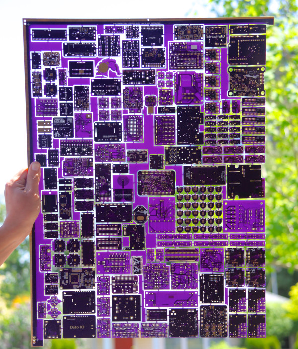
Panelizing boards is something most of us won’t have to do often. Really, you only want a panel of boards when you’re manufacturing something. For small-scale production and prototypes, bare boards will do just fine. Simply by virtue of the fact that panelizing boards is far less common than throwing some Gerbers at OSH Park or Seeed, there aren’t many (good) tutorials, and even fewer (good) tools to do so. This is how you panelize boards quickly and easily using Open Source tools.
What I want
Panelizing boards, or putting multiple copies of a board in a single Gerber file, is nothing new. We’ve seen it done in Eagle with a ULP script, and we’ve seen it done in KiCad with some Python. [Dave Jones] did a panelization tutorial for Altium. All of these have their downsides. Putting more than one board design on a panel is not covered by the usual tools and tutorials. Most methods of panelizing boards only work with rectangular boards. Altium will do anything, but Altium is pricey.
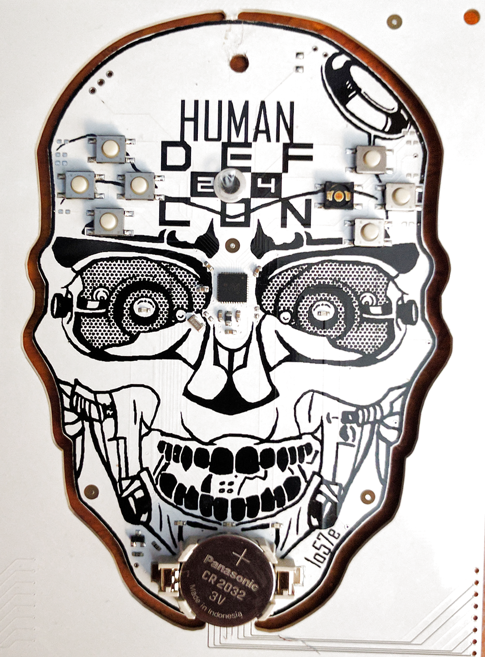
What I need is a method to take more than one weirdly-shaped board, and put it on a rectangular panel. Need an example of this? Check out the DEF CON 24 badge to the right. This is a weird-shaped board, designed to fit into a rectangular panel for automated assembly. Instead of v-grooves, the board is simply milled out of the panel, held on with mouse bites, or small tabs of fiberglass and holes. Extremely clever implementations of this technique also allow for pads and traces on the panel for programming each individual board.
Can you do this in Eagle and KiCad, the most popular tools for low-scale PCB design and fabrication? Yes, but it’s hard. Altium will do it easily, but that’s really a tool for people who are manufacturing tens of thousands of boards. To date, I’ve only found one tool that simply allows you to drop multiple Gerber files on a board and merge them.
Gerber Panelizer
The best tool I’ve found for panelizing multiple board designs with routing and mouse bites comes from [Stijn Kuipers]. His PCB Panelizer (available on GitHub) is the best thing I’ve found to take Gerbers you’ve already designed and turn them into an easily manufacturable panel. Before finding this fantastic tool, I spent about a day trying to figure out how to panelize Gerbers. After finding this tool, I was able to create the panel I needed in about twenty minutes. Gerber Panelizer is a fantastic tool, and I’ll be dedicating the rest of this post to the ins and outs of this simple and easy way to create panels of PCBs.
Using Gerber Panelizer
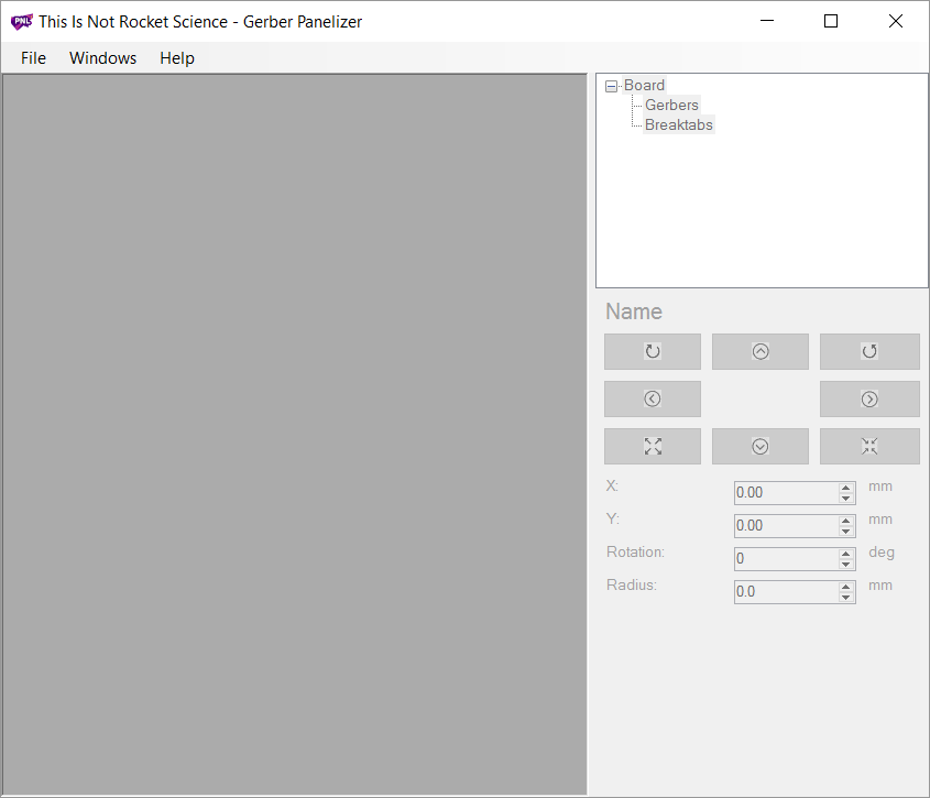
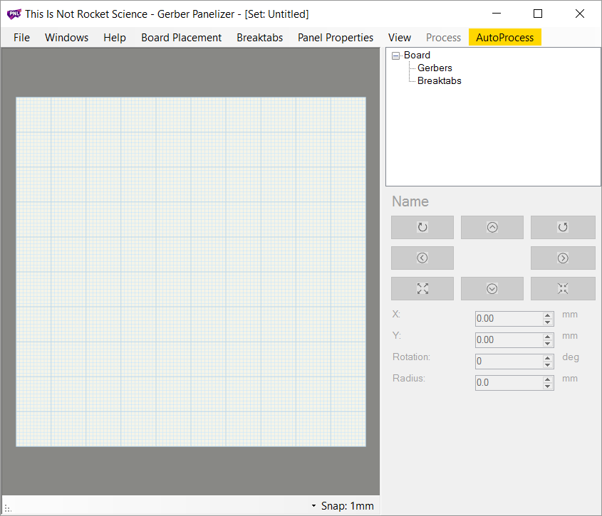
Using Gerber Panelizer could not be simpler. All you have to do is set up the size of the panel, drop .zip files of your Gerbers onto the panel, add some breaktabs, and export the merged gerbers. After your computer does a little bit of thinking, you get a panel of boards, ready to send to a fab.
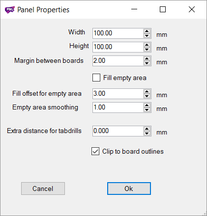


Of course, you’re not limited to square or rectangular boards with Gerber Panelizer. Any shape will do, and the ‘Fill Empty Area’ in the Panel Properties window makes creating panels of weirdly-shaped PCBs easy.
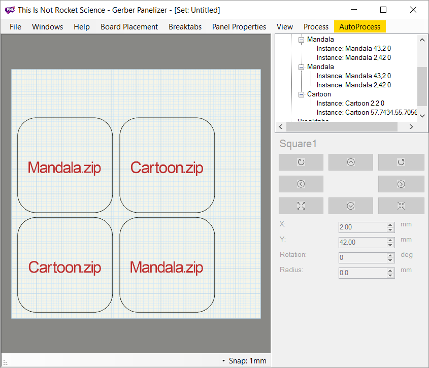
I whipped up a quick artsy board of the GitHub Unicorn (five minutes in Eagle) and stole the source for the Freeduino. This is the best example of what Gerber Panelizer can do. With this tool, you can panelize oddly-shaped boards, and put more than a single design on a panel.

Caveats to Gerber Panelizer
Gerber Panelizer is a great tool that allows you to quickly and easily stitch multiple Gerber files together into a single, easily-manufacturable board. Unfortunately, the DIY PCB crowd and Open Hardware enthusiasts in general, are cheapskates. Conventional wisdom says the only tools worth having are the ones that are the ones that are free as in beer, an argument often transparently disguised as ‘free as in speech’. This means the software is offered without support, and often with broken features.
Gerber Panelizer is not without significant issues, although some of the blame can be directed at KiCad. The KiCad philosophy makes a distinction between milled, plated layers and the final cutout of the board. In KiCad, this means there’s a difference between .GKO and .GML Gerber files. KiCad, in its infinite wisdom, decided the cutout layer of the board should use the file extension .GM1 as an output Gerber. This has caused much confusion, but the good news is this issue will be fixed shortly. OpenGL on Windows with Nvidia drivers is a hot mess of a dumpster fire. This problem can be solved by using my laptop instead of my desktop battlestation. Additonally, the current release (at least at the time of this writing) does not support adding breaktabs between a Gerber file and the ‘fill empty area’ area. This was a bug solved by [Arsenijs] over on Hackaday.io. I owe him for fixing that bug for me, but the important thing here is that I contribute money to Open Source development.
Is this a perfect solution to panelizing PCBs? No. Ideally, you’d want fiducials along the edge of your panel so the pick and place machine can tell where in space the panel is. You’ll also want some M4 holes along the side of the board, so the pick and place machine can move it along the manufacturing line. However, this is quite literally the easiest and simplest way to panelize a bunch of boards. No other tool comes close to Gerber Panelizer’s ease of use.
Despite these issues, Gerber Panelizer is a simply fantastic piece of software that should be in everyone’s toolbox. Yes, there are issues, but it looks like the most critical will be fixed in the next release.
If you’d like to play around with these Gerber files, you can find them here on hackaday.io.


I’ve heard good things about http://www.downstreamtech.com/cam350.php but it’s certainly not free.
I work in a pcb fab house, and we use Cam350 to do all our panelization. We do the work manually, even when there is a panel editor in the software. I’m probably the only one capable of learning on how to use it, but I just don’t have time. The major downfalls in using the panel editor is that the working frames we use are not made in the panel editor to begin with. We just panelize the boards manually, and add frames to x0 y0 basicly, merging with the multiplied source material.
One of these days I’m going to go throught the feature with a fine comb, since it’s capable of fitting multiple boards in one panel automatically, although we don’t make multiboard panels. But it would be nice to atleast get the max amount of boards fitted with a press of a button.
I do this sort of work as well as gerber conversion, inspection, DRC, and cleanup in ViewMate from Pentalogix:
https://www.pentalogix.com/t/software-products/viewmate
Great tool and reasonably priced for both Deluxe and Pro tiers.
The board house I use gives me 4 boards [min] up to 60 sq in for $33/each, but throw another $50 lot charge at them and I get as many boards as I can fit in the 60 sq in, but I have to cut them apart myself – a pain until I found a 4″ tile saw at a garage sale – allow a 1/16″ gap between the boards, and the tile saw cuts them apart like butter [straight edges on the boards also. ] Putting the board with funny notches along the outside and the board shop routes that for me. I let the board outlines print on the solder mask layer and drill 1/16 holes on inside corners and use a nibbler to cut those. A bit of work, but then the cost drops to about 60 cents a square inch – not too shabby for an under 2 week turn.
I also like a tile saw for cutting boards – and a wet saw will keep the glass dust out of your lungs. The other nice thing is that a diamond blade doesn’t get eaten by FR4 like steel ones do. My 12″ sheet metal shear is in dire need of new blades after cutting too much of the stuff.
OSH 30 sq in.
The break even point (including the $50.00 step/repeat charge and shipping). ;)
Wow, my greater than and less than signs got removed along with the content between them, (must have been interpreted as HTML).
If less than 30 sq in, use OSH
If greater than 30 sq in, use AC
Some suppliers will do the panelizing for you. Usually at a price of course. :) But it can be handy if you don’t know things like the space between boards (incidentally, it’s 2mm for the Chinese board house I usually use.)
I use Altium at work, but I’ve only ever had a use for panelizing once. It’s kinda handy to only have to align and paste once for a set of boards, but most of my designs are roughly 20″ square (500mm^2) single boards, and it gets tedious to tweeze parts on multiple copies in one sitting.
If you are using eagle and want some control over it, I made a tutorial here: http://smdprutser.nl/blog/eagle-panelizing-made-easy/
I use this to combine small boards into the ‘standard’ el cheapo PCB 5×5/10×10 offerings by Dirtypcbs.com or Seeed
Thanks.
We usually order our boards for prototypes with Würth in Germany (wedirekt.de). They may be a bit pricey, but we always get top quality and sometimes need more complex boards (HDI, Micro Via, Burried Via) from them too, so we decided to get the more “standard” prototypes at the same place. In the online configurator you can set up panelization too, even decide on scored or milled or mixed outline or give them a drawing of the panel you want. Since we use Altium Designer we prefer to panelize in house tho, as that makes it a bit easyer for us to have full control.
As a general hint, ask your prefered board fab what size of production panels they run and adapt your design to maximize the use of that panel if possible. Of course, if you go thru a full automated production chain, make shure all involved machines like paste, pick&place, reflow, maybe even wavesolder and inspection work with your panel. For programming and circuit test you usually remove the individual boards from the panel first and then run these last steps.
Of course in the end it really depends if you want to or need to squeeze the last cents of profit out of your production run or not….
Doesn’t make sense to use Würth for standard boards. 10 boards, 10 cm x 10 cm, costs EUR 309.52 (with the longest option, 5 working days, EUR 6.90 shipping included) at Würth. The same costs $16.90 at seeed studio ($12 shipping cost included). That’s 15 times more expensive at Würth! And you can use faster shipping at seeed, if you need it fast, and it would be still multiple times cheaper.
Compare Oranges with Bananas, and you get to your results i guess. When i set seedstudio to the same spec as the boards i would order from Würth, i basically get pretty much the same price for both (fusion PCB not fusion PCBA).
Shure, if you choose the cheapest possible option available, seedstudio beats Würth by a landslide, but once you level the playfield, they all cook with the same water. And the cheapest possible option we can do in house with our own etching station anyway, so we would not order these boards online. On top of it all, i’d rather pay a bit more and keep the money in my country and keep some jobs in europe, instead of cheaping out completely with asian suppliers and then cry around that all the jobs in maufacturing get transferred to asia.
Right, but you are missing the point that you can’t lower the specs if you order at Würth. And paying more for PCBs just to keep some jobs in Europe doesn’t make sense either. I could argue that if you pay more, your products are more expensive, so less customers will buy it and your company might go bankrupt. You might not like it, but the philosophy of capitalism is to buy the cheapest, if the quality is the same. Global trade is good for everyone.
If we order boards at Würth online thru wedirekt, these are usually just a handful of prototypes anyway. Paying 100€ or 500€ for a few boards really does not change the end product price for our customers in any way, as we work with development budgets beyond a few 100k$ for our products from prototype to fully certified end product. Of course, once the designs are industrialized and in series production, none of these panels get fabbed in the expensive prototype facility of Würth anymore…
And to your last sentence, that might be true, we tryed to get the same consistent quality from other surces, and unfortunately, if you go with the cheapest option every time, it’s a hit and miss game. Debugging/fixing badly produced boards is not free work either and something we rather not worry about in the prototype stages where you could on top of it have other problems/errors in your electrical design too.
The point that global trade is good for anyone is something i would disagree on (pollution, exploitation, waste of ressources,…) but thats not the topic here i think.
I like OSH Park very much and have used them since they were called DorkbotPDX but sometimes I also like to use SeeedStudio and Smart Prototyping, which are faster and offer white solder mask with black silkscreen. SeeedStudio includes a small code on each board though. Both charge extra for ENIG but I find HASL easier to solder to anyway.
Relevant because both SeeedStudio and Smart Prototyping de-panel leaving a smooth finish so I don’t have to post-process as I do for boards from OSH Park.
OH MY GOD YOU PUT IN A DICK BUTT. YOU FILTHY CRETIN!!!
I SEE A 9GAG PEASANT!
I’ve only done small PCB panelisations, and by hand in KiCad…
I had a similar problem recently though where I had to manufacture a whole kitchen full of cupboards on my CNC router. 8 cupboards, each with about 13 panels of wood (drawers!), each with its own specific machine-ops (drill holes, countersinks, hinge pockets, biscuit slots, etc) … and they all need to be relatively-efficiently packed into 8×4′ sheets.
I ended up writing a pile of Python (because CamBam) to do it all, but by god it’s stinky (parseltongue is not my native language). I should put it on github but I don’t know whether people would be more grateful for its use or offended by the code quality…
Is there any good free panel-packing software out there for not-PCBs? Including some optimisation and/or rotation tests? That will combine the G-code for each MOP on each panel into a set of G-code files for each sheet?
I can so agree on the OpenGL dumpster fire comment. But, hey, at least the dumpster fire is portable… ;)
Where panelization really makes sense is when you have multiple designs going out to an assembly house. Board area costs are a drop in the bucket compared to setup/NRE costs for both fabrication and assembly houses. I’m currently working on a project that is split into 6 different PCB assemblies, and by moving each $1500 design into a single panel, the total cost went from $1500 x 6 = $9000 to about $1900 for the whole project (mostly due to a costly BOM). Even when factoring the hour or so that it took to setup the panel, $6-7k is some pretty good savings. I don’t think it’s worth it if you plan on nailing the prototype in one or two revisions, but for a heavy-duty R&D project, it’s nice to get your monthly prototyping cost down.
Altium’s embedded board feature, when used with different designs, doesn’t play nicely with assembly houses, as it doesn’t have any ability to magically fix duplicated component designators. So I ended up just copying-and-pasting the existing designs (after re-annotating them) into a new PCB document, unioning each design (to make it easier to delete/replace later), and separating with V-score lines.
Straight edges are basically a must for this method (so you can just V-score it). Otherwise, try to lock in your irregular board shape at the beginning and stick with it, as it will take quite a bit of time to draw the mouse bites and contour routing paths.
So, the zip file download doesn’t contain any .exe or installer. How do you install this tool?