Panelize PCBs Graphically With Hm-panelizer

When you’re working with PCBs and making single units to knock out in those Chinese fabs, going from layout to manufacturable Gerber files is just a few button presses, no matter what PCB layout tool you prefer. But, once you get into producing sets of PCBs that form a larger system, or are making multiple copies for efficient manufacturing, then you’re not going to get far without delving into the art of PCB panelization. We’ve seen a few options over the years, and here’s yet another one that’s looking quite promising —  hm-panelizer by [halfmarble] is a cross platform Python GUI application, which leverages Kivy, so it should run on pretty well on most major platforms without too much hassle. The tool is early in development, so is restricted to handling only straight PCB edges, with horizontal mouse-bites for now, but we’re sure it will quickly grow more general purpose capabilities given time and support.

In an ideal world, open source tools like KiCAD would have a built-in panelizer, but for now we can dream and hm-panelizer might just be good enough for some people. For more choices on panelizing, checkout our guide to making it easy, and just to muddy the waters here’s another way to do it.

Panelizing Boards The Easy Way

For reasons that will remain undisclosed until some time in the future, I recently had a need to panelize a few PCBs. Panelization is the art of taking PCB designs you already have, whether they’re KiCad board files, Eagle board files, or just Gerbers, and turning them into a single collection of PCBs that can be sent off to a fab house.

Now this is panel racing

If you’re still wondering what this means, take a look at the last board you got from OSH Park, Seeed, Itead, or Dirty PCBs. Around the perimeter of your board, you’ll find some rough spots. These are ‘mouse bites’ and tabs, places where the boards are strung together to form a gigantic rectangular panel sent off to a manufacturer. You can check out this great interview with [Laen] from OSH Park to get an idea of how this works, but the basic process is to take a bunch of Gerbers, add tabs and mouse bites, solve the knapsack problem, and send the completed panel off to a board house.

Panelizing boards is something most of us won’t have to do often. Really, you only want a panel of boards when you’re manufacturing something. For small-scale production and prototypes, bare boards will do just fine. Simply by virtue of the fact that panelizing boards is far less common than throwing some Gerbers at OSH Park or Seeed, there aren’t many (good) tutorials, and even fewer (good) tools to do so. This is how you panelize boards quickly and easily using Open Source tools.

Continue reading “Panelizing Boards The Easy Way”

Altium Gives Away The Farm With New Circuit Maker Software

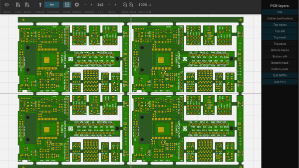
Things are about to get interesting in the world of PCB design software for the open source hardware community. This week, Altium launched the open public beta for its new Circuit Maker software, and it’s a major change from what we looked at previously. Everything is free.

You heard that right, free. Unlimited board size, and unlimited layers – all free. And this isn’t some stripped-down, bare-bones software here. They’ve thrown in almost everything under the sun; a 3D viewer, team project collaboration, EagleCAD and DFX import, integrated Octopart supplier and pricing information, no commercial usage limits, and project sharing. And if that isn’t enough, the “engine” seems to be the exact same back-end that is used in the full $10,000 Altium Designer as well(with a bit easier to use user interface on top). This is a major departure from the pre-beta we covered back in September. Altium was going have board size and layer limits, with the ability to “upgrade” at a cost. So by now you’re thinking to yourself “OK, what’s the catch?” Well there are a few gotchas – but only a few.

The software uses cloud based storage for your project files, and is community based. It won’t work without an Internet connection, there is no local storage, and it forces you to share your projects with the world. You do get two “Sandbox” designs that you can hide from the world before you generate your gerber files, but after that, your project is online for the whole world to see. Will that be a deal killer for the OSHW community? We’ll find out soon enough.

One thing is for sure, anyone with a doggy Internet connection is not going to enjoy using Circuit Maker (we’re hoping they remove that limitation in the final product). And as with any cloud based service, we wonder how many people will be willing to trust their designs to a free service that could be turned off on a whim? Or will the unlimited board size and layers, combined with Altium’s name and robust software win people over in the end?

If you want to see in-depth review of Circuit Maker, we highly recommend you watch the video after the break.  [Dave Jones] of the eevblog, gives you a full rundown on the beta version. Dave’s in a unique place to review this software, not only has he been using Altium since the mid-80’s as a professional engineer, he’s also a former Altium employee.

Continue reading “Altium Gives Away The Farm With New Circuit Maker Software”

How-to: Prepare Your Eagle Designs For Manufacture

back

Cadsoft Eagle is a multi-platform freeware circuit layout program. Lots of open source hardware is designed in Eagle, and it’s become a hobbyist favorite. We use it for all of our hardware designs.

There are several ways to turn an Eagle design into an actual printed circuit board (PCB). We’ll show you how to save Eagle designs as industry-standard gerber files that are accepted by any PCB manufacturer. You can use the gerbers to order a single prototype, or a full panel.

Continue reading “How-to: Prepare Your Eagle Designs For Manufacture”