If you are even remotely interested in electronics, chances are the number ‘555’ is immediately recognizable. It is, after all, one of the most popular IC’s ever built, with billions of units sold to date. Designed way back in 1970 by Hans Camenzind, it is still widely available and frequently used for various applications. [Ken Shirriff] does a teardown and analysis of a 555 and gives us a look at the internal structure of this oldie.
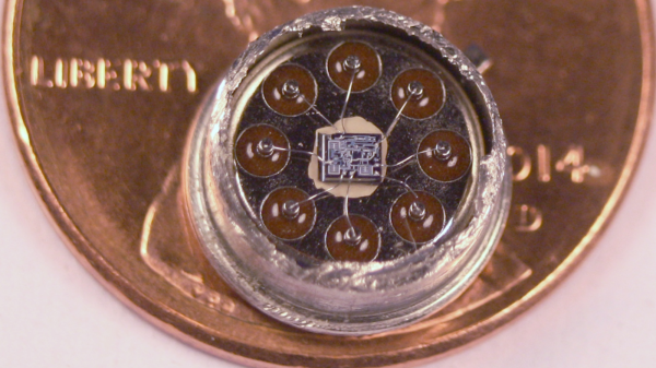
A metal can package allowed him to just chop off the top and get access to the die, which was way safer and easier than to etch out the black epoxy of a DIP package. He starts by giving us a quick run down on how the chip works, showing us the two comparators, the output flip-flop and the capacitor discharge circuitry that make up most of the chip. He then puts the die under a metallurgical microscope, and starts identifying the various sections of the chip. Combining pictures of individual elements with cross-sectional diagrams, he identifies the construction of the transistors and resistors, the use of a current mirror to replace bulky resistors, and the differential pair that makes up the comparators.
He wraps it up by providing an interactive map of the die and the schematic, where you can click on various parts and the corresponding component is highlighted along with an explanation of what it does. There’s some interesting trivia about how a redesigned, improved version – the ZSCT1555 – couldn’t survive the popularity and success of the 555. He wraps it up with a useful list of notes and references. While de-capping blog posts are interesting on their own, [Ken] does a great job by giving us a detailed look at the internals.
Thanks [Vikas] for sending in this tip.


