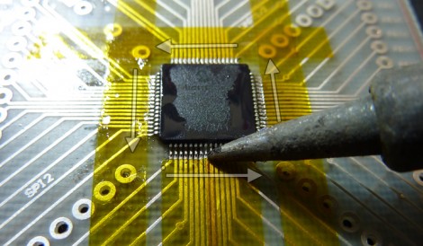
Drag soldering works exactly as its name implies, by dragging a bead of solder across fine-pitch pins you can quickly solder an entire row. The method relies on clean joints, so liquid solder flux is often used to make sure there is good flow. But if you’re drag soldering on boards that you’ve etched yourself the solder can sometimes run down the trace, rather than staying where you want it. Professionally manufactured boards don’t have this problem since they have solder mask covering the copper that doesn’t need soldering. [Ahmad Tabbouch] has a method that uses Kapton tape to act as a temporary solder mask on diy boards.
The process involves several steps. First, three strips are place horizontally across the board, leaving just a portion of the upper and lower pads exposed. Those pads are then tinned with solder, and a light touch with an X-acto knife is then used to score the tape covering the vertical rows of pads. Once the waste as been removed, two more strips are added and those rows are tinned. From there the chip is placed and soldered as we’ve seen before; first tacked in place, then fluxed, and finally drag soldered to complete the connections. This achieves a crisp and clean connection, presumably without the need to clean up your solder mess with solder wick.
Kapton tape resists heat, making it perfect for this process. We’ve also seen it used on hot beds for 3D printers, and as a smoothing surface for sliding mechanisms.
[via Dangerous Prototypes]


Usually when I hear Kapton I think of flaming aircraft falling from the sky. Good to see it put to good use.
kapton has been used for thermal insulation since the Lunar Module landed on the moon. good to see its become a bit more available to the average hacker.
Kapton makes a great solder mask, I have been using it for years. also you can get it from uline for fairly cheap.
Awexome idea!
you also see it used in SMPSs as well, and a few old laptops used it to hold the CPU traces for the flip chip in place.
Ought to be reuseable though.
Haven’t read the article yet, but what bothers me about the picture is the insanely oversized soldering iron tip. If you’re doing surface-mount parts, nifty tricks do not make up for not having some of the baseline appropriate tools.
As far as the usage of Kapton tape, I ran in to a couple situations recently where it saved my bacon:
In one case I had put un-capped vias (since the DorkbotPDX group order doesn’t do microvias or capped) underneath a USB micro-B connector, before I realized that the metal shell of the connector was flush with the surface of the board… It ended up soldering the vias together, which was bad. A bit of Kapton tape over the vias worked nicely, though it raised the part up enough that sometimes the main pins wouldn’t solder right.
The second case involved a chip that was narrower than the footprint on the PCB. Vias just inside the pads would solder to the pins because of the position of the chip, and a number of the vias were offset enough to solder to the next pin over… Again Kaptop tape to the rescue.
I’ve checked Digikey for the tape with no success, but as it turns out I had a decent supply of it in the form of the little squares stuck to the top of various USB mini-B connectors on my various projects. Presumably it’s put there to avoid getting solder inside the connector during (I’m guessing) wave soldering, but it sure came in handy…
Yesterday though I tried a new technique: a Sharpie. A couple “coats” of ink over the vias provides enough “solder resist” to keep the case from shorting them out, at least under the USB connector. I’ll be trying it out on the too-narrow chip here in a few minutes.
i did this a few times using regular paper masking tape. kapton tape would obviously be better though, but i’m pretty sure that every body has a roll of painter making tape lying around.
omegacs: there is nothing wrong with the size of that tip. I regularly solder finer components with thicker tips. After all, it’s not the size that counts, it’s how you use it :)
In fact, super fine tips do not work very well for drag soldering. Wide chisel tips are great.
Also, I think you’re confused about the difference between capped and tented vias. Tenting is where you have soldermask covering the via, capping is where you have copper covering the hole in the via.
Hm. I’ve noticed this happening before when I drag solder (or really with any type of soldering) but it’s never been a problem at all other than that it looks ugly. I’m assuming that this only becomes a problem when you’re not using a proper drag soldering tip (the kind with a bowl reservoir thing at the tip). I almost exclusively use this technique now, but I’ve never really gotten it to work with normal tips (probably because I’m not 1337 enough and am too lazy to do it the hard way =P).
@omegacs, drag soldering is the technique they actually have been using in industry for any hand-soldered multi-pin surface mount part since the 80s. I actually read about it in a soldering reference book from the 80s in the library before this technique appeared online. I’m actually a little surprised how little documentation there was on this topic about five years ago or so. The drag soldering tips are always much larger than the pins themselves–this allows you to solder more pins at once, and provides space for the solder reservoir on the tip. Trust me, once you try drag soldering (at least with a real drag soldering tip) you’ll never turn back for anything larger than an 8-pin op amp.
Oh, another REALLY cool thing you can do with a real drag soldering tip (mentioned in that same industry soldering book): if you empty out the reservoir, it works in reverse and you can actually clean up solder pads or remove bridges just by touching them or dragging out the bridge short. It’s REALLY convenient–even if you mess up, you can fix it in 2 seconds without pulling out the wick or any other nonsense.
Drag soldering FTW. I’d like to second what mjn and threepointone said. That tip isn’t too big. I used to think that a really fine tip was necessary for SMT work, but it isn’t. The place where I worked last summer used fairly large tips, which horrified me at first. Until I was shown how to drag solder…instead of soldering individual pins. It is much faster and the temperature of the tip doesn’t drop. I found that was an issue with smaller tips. And with some flux bridges are easy to remove with a dry iron tip.
i posted this 2 days ago on the forums
good to see it here as well
I lack to see how the tape helps any bit. Maybe I just have the right tools, but I have drag soldered endless amounts of SMD chips like the one in the pic and have not needed kapton tape at all. Using the tape for that reason is a little bit of a waste. Instead just purchase the right tools from the get go and there is no issues
great stuff!
the kapton on usb connectors and other components is for pick-place machines btw. it’s there that the vaccuum nozzle can grip it.
DeadlyFoez: the point of the kapton is for it to essentially act like your soldermask on a home made PCB. If you are having your PCBs commercially printed with a soldermask layer than there isn’t much of a need for the kapton (I guess it could be useful for protecting nearby components if your layout is super tight).
It’s creepy when things pop up in your daily browsing that you’ve been thinking about just days earlier. My reason for thinking about doing just this was more cosmetic though since I haven’t really had a problem with the actual soldering. I wanted to get crisp clear “edges” on the solder joints and judging by the pics that’s exactly what you get. Sweet!
Interesting that I’ve been using this method for many years, but have never heard of it called “drag soldering” before now. Maybe I need to get out more….? It really impressed my classmates in EE courses when I could solder MSOP and TQFP stuff with tiny pin pitches, and I didn’t even use tape. However, I did find the value of a high-quality flux pen, as well as its relatively sparse usage requirement for the best-quality joints.
Incidentally, since Kaplan tape is great as a temporary solder mask, is it possible to obtain sizable sheets of the material? I’m thinking I could send it through a printer (I have both laser and ink jet), print the solder mask template onto the sheet, and cut out the patterns as needed before applying. I wouldn’t even care if I had to apply the adhesive. Methinks this would greatly speed PCB prototyping. :)
Crap….KAPTON tape, not Kaplan….sheesh….
@omegacs: McMaster-Carr is a great resource for some hard-to-find materials. http://www.mcmaster.com/#polyimide-%28kapton%29-tape/=bq0fr4
I don’t know how their prices compare, but they have no minimum order.
dug up this to visualize to myself what was going on: http://www.youtube.com/watch?v=t06malVew40
That’s not a video, Now THIS is a ViDEO! ;-) http://www.youtube.com/watch?v=5uiroWBkdFY
more like Kapton tape: AIDS, in drag. amirite?
Damn, I never thought of that. I’ve tried drag soldering before, even have a nifty precision bevel tip with a little solder reservoir on the end. And yeah, on DIY boards, the solder’ll wick up and down traces all over the place.
Can’t wait to try this. I just happen to have scored like a dozen rolls of 3M kapton tape from a liquidator on eBay a year or two ago for almost nothing. :D
Maybe now it’ll see some actual use… ;]
I get my Kapton take from DealExtreme… *extremely* cheap:
http://s.dealextreme.com/search/KAPTON
Stuff works great!
Wow, cleaning his iron tip would help too! It’s so dirty that he may even need a new one…
@Faelenor
Hah in all fairness, it was a couple of years back and the tip had one good side to it :-P (didn’t use it much, most repairs were done at work); camera also makes it look worse than it really is
@Alex
You beat me to it, I was about to recommend DealExtreme! Their supplier (WLTape) also offers brilliant pricing for decent quantities
@omegacs
The little squares of Kapton tape on top of the mini-B connectors are for one reason – automatic pick&place machines.
Those devices work by using little suction pipes – the component literally gets sucked up from the ribbon feed, and is transported to the placement location while being held by the vacuum.
The Kapton tape makes it possible to hold the component against the business end of the vacuum pliers.
this sort of tape is used in pcb manufacturing to mask gold fingers prior to hot air solder leveling, among any other uses we can find for it. it works nearly as well as solder mask for fairly simple applications.
Good to see the soldering iron in the photo has an immaculately clean, tinned tip, ready to solder the IC.
Great idea about using polyimide tape to assist soldering. Thanks Ahmad.