It’s not uncommon to bitbang a protocol with a microcontroller in a pinch. I2C is frequently crunched from scratch, same with simple serial protocols, occasionally complex systems like Ethernet, and a whole host of other communication standards. But VGA gets pretty tricky because of the timing requirements, so it’s less common to bitbang. [Sven] completely threw caution to the wind. He didn’t just bitbang VGA on an Arduino, but he went one step further and configured an array of 7400 logic chips to output a VGA signal.
[Sven]’s project is in two parts. In part one, he discusses choosing a resolution and setting up the timing signal. He proceeds to output a simple(-ish) VGA signal that can be displayed on a monitor using a single gate. At that point only a red image was displayed, but getting signal lock from the monitor is a great proof of concept and [Sven] moved on to more intricate display tricks.
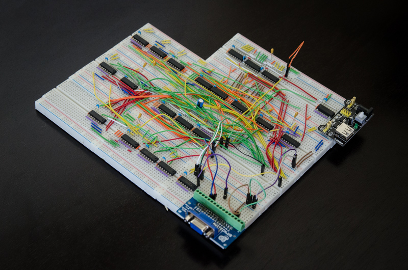
With the next iteration of the project [Sven] talks about adding in more circuitry to handle things like frame counting, geometry, and color. The graphics that are displayed were planned out in a simulator first, then used to design the 7400 chip configuration for that particular graphic display. It made us chuckle that [Sven] reports his monitor managed to survive this latest project!
We don’t remember seeing non-programmable integrated circuits used for VGA generation before. But bitbanging the signal on an Arduino or from an SD card slot is a great test of your ability to calculate and implement precise timings with an embedded system. Give it a try!


Now this is what you call a hack!!!
doesnt every single one of those discreet logic computers have some kind of video signal generator like this? what I find cool is that he has programmed the geometry and animation with discreet components too
The very early computers had a discrete chips video generator. Not long after computers started coming out with ASIC (single chip) Video generators, these still needed to interface to lots of memory chips and the CPU bus. The clone computers couldn’t clone the AISC or were in a different region and so needed different timing anyway so they turned to discrete chips.
The earliest Video chips were called Cathode Ray Tube Controllers (CRTC’s), a good example would be a 6845. Not long after, home computer manufacturers realised how important graphics were for the user experience (like games) and started making their own ASIC’s. The graphics quality and usability was the battle ground in the early home computer days.
It’s very interesting to see what early custom graphics cirquits were capable of, though. One computer I have with a custom 74xx based graphics cirquit has an up to 16-ink palette, 256 possible colors and a maximum resolution of 1024×256 (allthough then only with 2 effective palette inks). Considering the machine came on the market in 1984, those specs are not too shabby.
The limmiting factor with that sort of graphics setup is that the CPUs of the time were really too slow to use it well, and this particular machine has vertical scroll in hardware to at least prevent scrolling with text from being bog-slow.
This is very cool and quite nicely done! However, perhaps not the first such project. :-) http://hackaday.com/2011/10/06/a-masochistic-video-card/
Seems like this could be the first step on your way to building something insane like http://lucidscience.com/temp/vt93l.jpg (Vulcan-74 http://forum.6502.org/viewtopic.php?f=4&t=3329 )
These look amazing and painfully complicated.
The vulcan-74 isn’t just creating VGA video. It overlays numerous sprites on a playfield with adjustable offsets. I believe it also has some BLIT logic built in.
Yeah its pretty cool, this is the sort of thing I would love to do just for the fun of it, It’s amazing to see how small dedicated chips work on a breadboard it breaks it up so you can understand it easier.
It’s amazing! After reading about for a while I found myself on ebay just about to order a big batch of bread boards. Unfortunately – just as I was about to click ‘Buy Now’ – my left hand picked up a pencil and started stabbing my right hand holding the mouse!
Good decision. Plastic breadboards are a total waste of time for anything over three chips. Any more complicated than that, and you end up spending more time trying to troubleshoot the wiring than the circuit. I can wire a “deadbug” or perfboard project almost as fast as doing a breadboard, and have a good chance of having it work. I spent a couple of days trying to fix intermittent problems on a 20 MHz AVR-based project on a breadboard, only to discover eventually that stray reactance was causing it to oscillate at 60 MHz randomly. Transferred the circuit to perfboard and didn’t have any more troubles. JUST SAY NO!
Yeah, I’ve done four different projects that generated VGA output for various types of monitors, using 74HC or 74LS series chips, but I never even CONSIDERED doing a hardware blitter for any of them. That to me is the really impressive part of this.
The “masochistic video card” is somewhat misleading: although the timing is set up for an 800×600 resolution, it has only ONE pixel, which is the full size of the screen. Not impressed.
I see your point but I would be happy just to have it output something, Perhaps who ever made it went further eventually.
You didn’t read part two.
I don’t see any part 2. I see several pages of project description, going on to even making a PCB board version of it. It has no memory, therefore the whole screen is just one color at a time. Is there a part 2 somewhere else that I haven’t seen?
http://www.skrasser.com/blog/2015/10/08/vga-from-scratch-part-2/
I wasn’t commenting on this project. I was commenting on the “masochistic VGA” project that somebody else linked to.
It’s actually 800×600 repetitions of the same pixel that is one color from a range of 8.
If you had done this before then you would know that getting to this stage is the hard part and the rest is relatively easy.
I’ve done this recently, and getting the sync signals was much less than half the battle! Admittedly, bitbanging it on an MCU, the timing must be challenging, but getting useful data in between those sync pulses (that isn’t one colour) is non-trivial!
I HAVE done this, four times that I can remember right off the top of my head, and this is the straightforward part. The hard part is multiplexing the memory so it doesn’t show glitches on the screen every time the CPU writes to screen memory, and getting the timing right on shifting the bits out.
Well that’s probably why I used the term ‘relatively easy’ and not ‘trivial’.
Sure sync is easy but the project does specify an exact non-binary resolution so the counter chains must be completed to.
I have also done (or doing) this in VHDL / CPLD here –
https://hackaday.io/project/3610-z80-retro-computer-with-graphics
and here –
https://hackaday.io/project/5565-trs-80-compatible-clone
@[BrightBlueJim] I would be interested to see how you dealt with the CPU access ‘glitches’
Ah I missed your comment on Vulcan-74 and made my own about it. But yes seeing this article claim this to be the first brought Vulcan-74 to mind. I actually bought the SRAM for the project and started to WIRE WRAP my own similar project. Just haven’t had the time though :(
Isn’t that how IBM originally built the first Video Graphics Array boards?
I remember the IBM CGA card and it was covered in 74xx TTL chips *but* it also had a 6845 as well so it wasn’t technically discrete chips as the 6845 was a CRTC.
I did see lots of early VGA – SVGA boards but not from IBM. They all had some form of graphics processor. VESA came in as a standard with SVGA (or was it VGA) and had a lot of hardware requirements that you just couldn’t fit into a board full of TTL.
I tried that a LONG time ago and failed miserably. Congrats Sven, good job.
By the time VGA arrived, nope. We implemented VGA straight from simulation to silicon. VGA was developed with four releases of chip to the fab – the designers released a chip with the core interfaces on first, then added additional features in the next pass and so on, until pass 3
However, in the late 70s / early 80s, we designed color graphics displays by designing the LSI, simulating it and then using ‘sunburst’ cards, where each chip in the eventual machine was prototyped in TTL on a board. The LSI chips had about 100 or so gates each, and the sunburst cards held up to sixty TTL packages. The software used to generate the TTL boards from the LSI design could only support simple gates – NAND, NOR and inverters.
We built the IBM 3279 prototypes in this way – a big, hairy machine with a number of motherboards, each representing a single PCB in the final machine; each motherboard had a number of boards plugged in, each board representing a single chip in the final machine. The first boards were TTL, and then as the chips came back from the fab plant, the first step would be to put a single chip on a board, and replace its TTL version with the version on a chip.
Got any pictures?
Thanks for sharing this [Nick Sargeant]. I started with PC maintenance shortly after this – around the time of the XT.
Facinating! I am always interested in how they prototyped in the “olden days”. Please tell us more?
Seconding for pictures! Do you have kept any of the hardware? I have a few bits and pieces of prototyping hardware from the companies I have worked at.
“Spit Out VGA with Non-Programmable Logic Chips”
Wrong. These chipped ARE programmed, by a human placing wires on the breadboard.
No, that’s not what programming is.
Someone using electronics to do what electronics do!? Say it isn’t so!
I mean, first people were using tubes as gates, and then transistors as gates, and then those transistors were integrated and then integrated further, so someone took a step backwards and used logic ICs to do something that is now done on chips with further integration.
It’s not like, impossible, it just takes a lot of logic chips and jumper wires.
When someone does VGA with tubes, wake me up.
And like, how many times have we seen this done now?
Relays. Show me a VGA implemented in relays. It’s okay to have a really slow clock. And maybe a refresh rate of a day or two.
You’d get a sound card for free too! :-) The noise of relay-based shift registers and counters must be epic…
“We don’t remember seeing non-programmable integrated circuits used for VGA generation before. ”
While I highly commend these ultra bare-metal retro projects all the time *** I am all for it *** that quote from the article is >>>very<<< misleading.
Anyone who was born before the internet knows very well this has been done before.
This type of design was done countless times in the 60s, 70s, 80s in mainframes, minicomputers and even arcade machines.
So we didn't exactly have VGA back then, 800x600x16millions colors, but they came close sometimes. The same theory, principle, etc applies in the design which exists in this project.
Again, kudos to the hacker/maker for making this project. I'm all for showing that retro-hacking is a great hobby. Also, showing what is still possible today with that technology is always welcome.
Born in the Retro-USA,
Dan
[can’t find the edit button]
I neglected to say regarding that quote from the article,
there have been recent projects from others as well using the ultra bare-metal retro hardware for VGA projects.
I know you can google it – I have it buried in my bookmarks still.
Excellent point. This build qualifies almost as a simulacra, considering hardware of the era that first implemented VGA wouldn’t have been doing it with pure TTL. Yet it simulates something that *might* have been, under the right circumstances (it’s not like these parts were unavailable).
Also, strange coincidence, Dan: I’m wearing a t-shirt you designed right now…
You are correct, this guy did it before. And his was a HUGE project, still ongoing from what I know.
http://forum.6502.org/viewtopic.php?f=4&t=3329
https://www.youtube.com/user/LucidScience
For example, here’s the Williams Defender (1981) “theory of operation” manual, which has an excellent all-discrete video board, and a nice schematic of which bits do what. There’s a really nice one for the Q*Bert original schematics on youtube too, done by someone who re-implemented it all in FPGA.
http://www.arcade-museum.com/manuals-videogames/D/Defender.pdf
Ahh Defender a favourite from that era. Oh course you five digited humans could never play this five button beast!
I can still hear the game start sound if I want to.
A lot of early microcomputers such as the Apple ][ and TRS-80 model I and the Cormenco Dazzler generated a video display with discrete logic and maybe a character rom.
That’s right – I remember studying Wozniak’s state machine design for the video output, which if I remember correctly, could generate either PAL or NTSC compatible signals, using just a few TTL gates and flip-flops. It was a work of art. Whoever said that NTSC video is more forgiving than VGA never had to deal with color carrier phase or interlace. The Apple ][ didn’t generate interlaced video, but I’ve had to deal with a monitor (a Sony Watchman “flat” CRT) that wouldn’t behave correctly unless you gave it two 262.5 line fields. I had to implement two counter chains – one to count lines for the RAM addresses, and the other to count half-lines for sync generation.
And thank you for mentioning character ROM. Much of the innovations in video displays in the 1980s came not just from the limitations of CPUs, but also from the cost of RAM. The designers chose the size of RAM the budget allowed for, and then got the most out of this using tricks like changing the timing and routing the signals differently to get “text” and “graphics” modes, where the text modes used the least-significant bits of the row counter to address the “row” inputs on a character generator ROM, and read the columns out of that using a shift register. Not for the faint-hearted. The legacy of those days lives on in modern VGA chips, which all have to implement character modes that are still used by the BIOS and in the boot process.
Another reason for using a character ROM was that it wasn’t actually a ROM, it was a combinationally encoded ASIC which was much much faster that a normal ROM. This meant that the character ROM could run at a very high speed spitting out dots while the rest of the circuitry only had to grab bytes at one eighth of the speed and that gave time enough for the old slow DRAM (about 120nS – 150nS) to access the next character number. This RAM speed bottle neck influenced a lot of the designs of the era.
Actually, what I was talking about was literally a ROM used in the 1970s and early 80s – a 2513 to be specific. This was a mask-programmed ROM developed for dumb CRT terminals (aka “glass teletypes”) like the ADM-3, and had upper-case characters only, although you could also get a lower-case version and switch between them depending on the character. It was a much later development to have the shift register built into the ROM.
wow, at an access of 450nS it’s definitely a ROM. It must have been very hard to design for.
Love it. One more for the solderless breadboard naysayers.
Nay! Nay! Nay!!! Nay more braedbards!
This is my kind of porn. Good work!
This is a really great build, but is there a schematic for it? I am completely ignorant in this field, but starting from extreme basics sounds like a great place to start. At least that’s the way I like to do things.
My colleagues were needing CT DRS CT-1040 last year and located a great service that has a ton of fillable forms . If you are interested in CT DRS CT-1040 too , here’s http://goo.gl/1HCTiJ
Nicely done! Next challenge: add sound and enter it in the Wild competition at a demoparty. :)
Uh no this is definitely not the first time…
This is either the second or third time depending on how you count it.
Someone has already done a SERIOUS VGA 7400 series video generation system…
Sprite system and everything. All 7400 series and some SRAMs.
This guy did a whole system once then ripped it all out and started over again since something in his design changed.
His project is very very well done.
Check it out:
http://forum.6502.org/viewtopic.php?f=4&t=3329
https://www.youtube.com/user/LucidScience