An ordinary integrated circuit is made of layers of material. Typically a layer is made from some material (like silicon dioxide, polysilicon, copper, or aluminum). Sometimes a process will modify parts of a layer (for example, using ion implantation to dope regions of silicon). Other times, some part of the layer will be cut away using a photolithography process.
Researchers at MIT have a new technique that allows super thin layers (1-3 atoms thick) and–even more importantly–enables you to use two materials in the same layer. They report that they have built all the basic components required to create a computer using the technique.
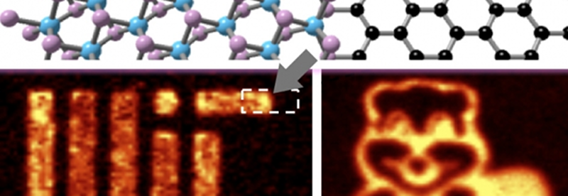
The prototype chips use two materials: molybdenum disulfide and graphene. The method apparently works with materials that combine elements from group six of the periodic table, such as chromium, molybdenum, and tungsten, and elements from group 16, such as sulfur, selenium, and tellurium.
To assemble their integrated circuits, the researchers first place a layer of graphene on silicon. Then they etch the regions where they wish to deposit the molybdenum disulfide. Next, at one end of the substrate, they place a solid bar of a material known as PTAS. They heat the PTAS and flow a gas across it. The gas carries PTAS molecules with it, and the molecules stick to the exposed silicon but not to the graphene. Wherever the PTAS molecules stick, they catalyze a reaction with another gas that causes a layer of molybdenum disulfide to form.
We’ve seen a lot of interesting work on graphene for semiconductors and even things like capacitors. You have to wonder what graphene-based components we’ll be building with in the next decade.


SSD breakthrough?
Smaller arduinos’
#getHype
Faster LOLcats.
Are current ICs constrained by the thickness of the active layers, or by the thickness needed to hold together mechanically? Also, any word on component performance? This sounds cool but also a touch farfetched.
From the linked article:
“The new fabrication method could open the door to more powerful computing if it can be used to produce tunneling-transistor processors.”
Tunneling transistors, in short, can switch faster and with less current. From Wikipedia:
“The advent of a mass-producible TFET device…will enable the industry to continue the scaling trends from the 1990s, where processor frequency doubled each 3 years.”
Which processors haven’t been doing for more than a decade now. They’ve gotten faster mainly as a result of other improvements, including parallelism and task-specific optimizations; but which also make processors more complex.
So this might be very significant, *if* it turns out suited for cost-efficient mass production of TFETs with decent properties. “All the basic components required to create a computer” doesn’t mean much by itself. The same could be claimed of Minecraft, or strictly mechanical devices.
*if* it turns out suited for cost-efficient mass production” Always the real issue
https://youtu.be/tZeO9I1KEec
The second last paragraph is pretty much Ctrl + C, Ctrl + V. Would be nice if “quotations” were marked to know what is actual Hackaday content. Otherwise a link would probably be enough.
Thinner and smaller typically mean lower power.
And they will stop working when someone turns the light on, because of the intense photon bombardment of material three atoms thick :)
If you have lights that can shine through several tens of mm of glass filled dark epoxy (and the box it’s in), non-working ICs should not be high on your worry-about list :P
I like how when you click on the PTAS link, it reloads the page and brings you back to the beginning. It’s apparently trying to tell me to brush up on my reading comprehension skills because I obviously missed the first time around what PTAS is…
I was thinking PEETA from hunger games, but that doesn’t work here.
Is this kind of like what they do around 10 minutes in on https://youtu.be/tZeO9I1KEec ? Nanomanufacturing, flexible sensors, circuits printable on plastic
As cool as this is, i’d rather see a more research on how we check our chips without $millions in equipment. And how robust is material thats 3 atoms thick?
Is it just me, or does that look like a badger?
http://www.weebls-stuff.com/badger/video/badgers.html
In all seriousness though, using quantum tunnelling for transistors is a great idea, instead of trying to reduce the noise it’s making in contemporary designs.
Eh, how about a diamond substrate for high performance ICs first?