The current crop of ARM single board computers have a lot in common. Everything from the Odroid to the Raspberry Pi are built around Systems on a Chip, a piece of silicon that has just about everything you need to build a bare minimum board. You won’t find many hardware hackers playing around with these chips, though. That would require putting some RAM on the board, and some other high-speed connectors. Until now, the only people building these ARM boards were Real Engineers™, with a salary commensurate of their skills.
This is now about to change. Octavo Systems has launched a new product that’s more or less a BeagleBone on a chip. If you can handle putting a PCB with a BGA package in a toaster oven, you too can build your own ARM single board computer running Linux.
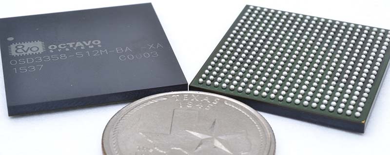
Octavo’s new System in Package is the OSD335x family, featuring a Texas Instruments AM335x ARM Cortex A8 CPU, up to 1GB of DDR3, and peripherals that include 114 GPIOs, 6 UARTs, 2 SPIs, 2 I2Cs, 2x Gigabit Ethernet, and USB.
The chips used in commercially available single board computers like the Pi and BeagleBone have hundreds of passive components sprinkled around the board. This makes designing one of these single board computers challenging, to say nothing about actually assembling the thing. Octavo is baking a bunch of these resistors, capacitors, and inductors right into this chip, allowing for extremely minimal boards running Linux. [Jason Kridner] – the BeagleBone guy – is working on a PocketBone, a full-fledged Linux computer that will fit inside an Altoids tin.
Of course, with this degree of integration, a BeagleBone on a chip won’t be cheap. The first part number of this family to be released, with the AM3358 CPU and 1GB of RAM, sells for $50 in quantity one.
Still, this is something we haven’t seen before. It’s a Linux computer on a chip that anyone can use. There is an Eagle symbol for this module. This is a chip designed for hardware hackers, and we can’t wait to see what people using this chip will come up with.


This is actually pretty cool. The large ball pitch should allow even a 2-layer board to work. I do wonder how well this package will handle thermals though. Will it crumble under full load? The datasheet is mum on the subject.
2 layer board is thing of the past. For a 20×20 BGA is at least 6 layers, event with large ball pitch.
That kinda takes it out of the “PCB in a toaster oven” difficulty range, doesn’t it?
Yeah, what she said, no
Probably you should buy a real reflow oven though – and get a stencil made and use paste
Depending on the application, the decoupling requirements (sounds like ma lot of that is already onboard), and the PC house layout rules (how tiny are those vias?) you might get away 4 layers, there’s no dram to route, don’t be tempted to putting vias in your pads
reading further, yes all the decoupling is internal, the app note says that no external decoupling required, that frees up routing space on thye bottom and around the edges and means you can potentially build a board with components on just one side.
In addition the power controller is also on the inside, that means you don’t need to hook up power pins, and as a result don’t need any planes, the grounds are nicely grouped, with (very!) careful routing you may be able to do away with a full ground plane as well – so yes, I think a 2-layer board is doable.
I downloaded the Eagle footprint, and hooked up the grounds – in DirtyPCB’s 2-layer rules there’s enough space to route 1 wire out between pads on the top layer and to drop minimal (.35mm) vias between pads – that means you can likely route out one wire on that layer too
(note there’s a row of grounds on one side that would be a routing block on the top layer)
Probably you can’t route everything out in 2 layers (you couldn’t build a beaglebone), you don’t have to route the DRAM so that’s probably half of the wires, you do have to hook up an 8-bit EMC (flash) bus
I’m kind of liking this for the core of a gigbit open source home firewall/appliance, esp. if 1000 of prices are a bit smaller
hmm… The PocketBone page linked in TFA says “2 layer board of 2.17×1.38 inches (55.02×35.03 mm)”. It may not do everything like break out every single I/O, but it does what the creator wants it to do.
I’m likely to agree that if you want a fully functional board with all of the I/O broken out, etc., you’ll probably need more layers, but to say that 2 layer boards are a thing of the past is naive.
My BS meter tends to peg all the way to the right when people speak in absolutes without regard to intent, ingenuity, or intelligence. It tends to show a lack of either depth of understanding or breadth of experience.
Thanks for playing.
Yeah, I believe Jason Kridner designed PocketBone to be a starting point in a free-of-cost tool (EAGLE) for people to make derivatives that use the new Octavo SiP. I’d like to get the design in Kicad, too, for those looking to designer bigger boards or use more layers.
The Octavo reference board design may be better for those that have OrCad and want to take advantage of all the peripherals that the BeagleBone Black has:
OSD3358 SBC Reference Design OrCad Files (RAR) | Version: B | May 3, 2016
http://octavosystems.com/octavosystems.com/wp-content/uploads/2016/05/OSD3358_SBC_RefDesign.rar
2 Layers?
Have you submitted a product like this to the FCC yet? Unintentional radiator with a clock above 9kHz, part 15 B.
Good luck with a 2 layer board.
Also, a toaster oven? How about an X-ray machine to validate that the BGA balls actually soldered properly.
The greatest thing about this system on chip is that it includes the power management system and the RAM. Hopefully this thing doesn’t get too hot when running full speed.
Please don’t invade their reality with logic. Silly Engineers are way overpaid…..
Everything high speed is contained within the package so 2 layer is fine. It’s the same as if you were designing a cape.
And you don’t need to x ray a 1.27mm pitch bga.
Do you guys actually make high pin count BGA products and skip AOI X-RAY?
What does IP-610 say?
Close your eyes, think happy thoughts and hope for the best?
I’m pretty sure most hobby projects don’t follow IP-610 or go for FCC certification. There are probably useful devices that could be made with this on a two layer board and home soldering, but they couldn’t be made to sell.
Unless you are in something like aerospace or medical, x-ray testing is typically only done on samples especially with such a large pitch part for process monitoring and improvement. There is just no need to x-ray every board. And if you don’t care about destroying your sample, you don’t even need x-ray. Just pry the chip off the board, or for greater visibility, apply dye first.
And here you are talking about hobbyists.
Everything except for all of the serial port PHY’s? Would you really route these without a ground layer beneath?
Don’t get me wrong, I think this is great and I can use something like this but the 2 layer advertisement… seems like a reach.
Gmii on two layers? You’ve got to be kidding!
If you are using high speed phys, you are going to need a 4 layer board. It’s not a big step up.
“Unless you are in something like aerospace or medical, x-ray testing is typically only done on samples especially with such a large pitch part for process monitoring and improvement. There is just no need to x-ray every board. And if you don’t care about destroying your sample, you don’t even need x-ray. Just pry the chip off the board, or for greater visibility, apply dye first.
And here you are talking about hobbyists.”
Sorry, I’m used to ISO factories making product for sale that meet assembly specifications. If prototype makers are the target market, then by all means ignore what i’ve said about AOI etc.
I think the PocketBone is aimed at people who want to use a EAGLE to create low-cost prototypes with batch PCB services. I know Jason would appreciate it if people forked PocketBone and created pull requests with improvements:
https://github.com/jadonk/PocketBone/
I think the Octavo reference design may be a better starting point for people looking to design a product: OSD3358 SBC Reference Design OrCad Files
http://octavosystems.com/octavosystems.com/wp-content/uploads/2016/05/OSD3358_SBC_RefDesign.rar
If you want to be sure all the balls soldered properly you will need to X-ray it. Even if you just reflow the BGA with hot-air the failure rate is very low. For a prototype you can solder it and hope for the best. If it doesn’t work try another one…
Most hackaday projects never get to the stage where FCC tests or X-ray verification are needed. If it works, it works; once it breaks, you try to figure it out and fix it, and if you fail, well, it is just a hobby.
Isn’t it more of a module than a chip? Sort of like a multi-chip module with epoxy encapsulation.
What is the big difference to the traditional processor & POP-memory approach with the RAM on top of the processor? The PMIC-chips and the passives?
TQFP package is about as small as I can practically design and make a PCB at home. I can’t image doing that with a BGA, how would one route all the inner pads to outside pins? Using multi layer PCB and vias? It’s probably easier and cheaper to get a PI zero if you have to break out the pins of the BGA chip, you’ll loose the compactness anyway. Maybe someone will get creative using the dead bug method on an epic (miniature) scale :)
You really don’t need to route very much depending on your application. And 1.27mm is seriously huge. We are talking 50 mil spacing. If your pad size is 20 mil, you can fit 2 traces between them at 6 mil design rules (20 + 6 + 6 + 6 + 6 + 6 = 50). That means on the top layer, you can escape the first three rows completely. You can then drop down some vias and escape the next 2 rows completely (27 mil via, 27 + 6 + 6 + 6 = 45). That’s 300 signals. You actually get more due to extra escapes on the corners. The module is 20×20, so that’s 400 pads. The module has far fewer than 300 unique signals, such as NC pads (55) and GND pads (80).
So no, you’d have no issues with a 2 layer oshpark board.
6 mil rules then breaking out and routing hundreds of signals on a 2-layer board is asking for trouble from a signal integrity standpoint. Never underestimate the value of (at-least) a ground plane in-between.
You’re better off with a BB Black or PI Zero unless you’re a wizard at routing and designing PCB’s.
Not to mention having a lot of experience with large BGA’s.
As far as a designing a two layer board goes for this monster chip, I’ll believe it when I see those who are promoting this idea do it for real.
There are far too many vaporware guys out there bragging they can do just anything with a two layer board and a oven yet I don’t so see no end product from them.
“If you can handle putting a PCB with a BGA package in a toaster oven, you too can build your own ARM single board computer running Linux.” — Oooooh.
“The first part number of this family to be released, with the AM3358 CPU and 1GB of RAM, sells for $50 in quantity one.”
That part seems to have 512MB of RAM
wow got to the site and look at the reference design, this “chip” is huge, somehow it remembers me of an old x486 processor,… don’t know why.
I’ve had a 486 chip on my desk for nearly 20 years. It’s more like half-dollar sized, larger than a quarter.
If this has the same level of support as TI’s other stuff I’m not touching it.
They offer two sources of support: A forum full of people just like you (also getting no support), and wiki which is a wasteland of half-finished pages and broken links.
Current project uses a TI SoC, if we realised when we started, well, we wouldn’t have started.
You have to know what you are doing before you start any embedded Linux project. I never used the TI kernel; just the mainstream. While I did run into SPI kernel issues it was nothing that couldn’t be fixed using, well, debugging skills.
No, really, he’s right.
Please explain when the babble USB error on the BBB gets fixed.
No, really, he’s not. I’ve developed products using the AM335X and the USB babble error has never been a problem. Complain to Gerald and not TI about the USB babble error.
I did.
It’s not fixed.
So this is a SiP (System in Package) right? co-located SoC, RAM, passive components, etc.
Or is it a SoC + PoP RAM? With passives around the outside, and then another pretty cap boxing it all in.
Finally!
PocketBone is a example of board with OSD3358, created in Eagle PCB with only two layer:
https://github.com/jadonk/PocketBone
Ironically, the BBB actually does fit in an Altoids tin.
It was (one of the ones I have, at least) even shipped in one.
They’re refering to the altoid smalls tins: http://jimdoran.net/joy/wp-content/uploads/2011/02/tiny-tin.jpg
So their goal is to produce a really small and useless Linux SBC that you really can’t do meaningful real world interfacing without adding a I.O board.
But it does run Linux. BFD.
This isn’t a hack, it’s just a form of “look what impractical BS I can make”
I think the PocketBone is meant to be a starting point in a free-of-cost tool (EAGLE) for people to make derivatives that use the new Octavo SiP. I’m hoping to get the design into Kicad, too, for those looking to designer bigger boards or use more layers.
The Octavo reference design might be better starting point for people looking to take more advantage of the functionality in the SiP:
OSD3358 SBC Reference Design OrCad Files (RAR) | Version: B | May 3, 2016
http://octavosystems.com/octavo_products/osd335x/
Anyone else tempted to deadbug it?
Tempting, but the result would more resemble a nice mold than a dead bug.
A breakout board version, pre-soldered [or perhaps sandwiched onto a sheet of pins] with a multi row dip or standard header style connection would be good though.
“…with a salary commensurate of their skills.”
Umm. Considering our salaries are similar to union sprinkler-fitter foremen, is that an insult?
Maybe you need a union, then.
“PocketBone”? Really? Surely he must have known the imagery he was invoking. Is he perhaps implying it is hard to use?
Now we just need a <$10 allwinner/rockchip/amlogic version
Amen. I’ve been looking for something cheap but useful to stick into a Dreamcast VMU https://en.wikipedia.org/wiki/VMU
Dual GigE ?
It seems like a good contender for a low power, high quality firewall?
How long until someone takes several of these and makes a SBC? As in, single board cluster.
It also supports SDIO so you could make it a router with wifi as well.
I wonder if the GPIO could be used to interface an SATA controler.
no need for SATA do what the BB does and boot from EMMC flash
Try saying that to a RAID controller
I remember thinking of this 2-3 years ago.
Yeah,
Mentorel, MYIR, etc. had a similar idea, but never got quite this small or at this price point.
Is ANYONE going to make one GAWD DAMNED REFERENCE of WHY? The Beagle Bones are Gud. Or Good? Ctrl-F “PRU” leads me to ZERO mentions of PRU’s. 55 comments and no mention. No mention of DAC or ACD speeds. No mention of BBBLue.
How much Malathion and Model Glue did some of these folks smoke as teens? Again. Let’s get the Non-Corporate Hacker rules straight. Since lisp-tweak speak is all the couture.
*Contribute a optimization or shortcut.
*Contribute a compatible extension.
*Point out a non-grammar nazi calculative error
*Suggest a possible workflow issue or work around
*Don’t shill, put down or elevate your “know-how” brand of crap.
https://s-media-cache-ak0.pinimg.com/736x/2d/69/62/2d6962311d038d10854fe208ffc397cb.jpg
Sorry, Unless you explode and scream we won’t hear you.
Why not use http://beaglecore.com/ instead?
With it’s footprint you won’t have problems with BGA fanout. It needs a bit more board space though.
Absolutely. We have started a project with a BBB and recently got our hands on the BeagleCore STEP files at GitHub (https://github.com/BeagleCore/Hardware) – it’s perfect for our needs. But I figure that there might be good reasons to use the OSD335x – but we wanted full compatibility and needed things like long-term availability as well as extended temperature range. And we like the LGA approach a lot. It just depends what you want to achieve.
I would like to see an even more reduced version in something like a TQFP144 package. BGA is still not the most tinkerer-friendly packages out there, while aTQFP can definitely be hand soldered on a 2L board.
If only they can multiplex the GPIO pins and make a TQFP144 version, bonus point if that version is pin-to-pin compatible with STM32F103ZE or ATSAM3X8E. (STM32F103ZE even have native pins for both SDIO/MMC and external RAM interface, which can be used to implement external storage and RAM for the BBB-on-a-chip)