Because I often work with students, I’m always on the look-out for a simple CPU, preferably in Verilog, in the Goldilocks zone. That is, not too easy and not too hard. I had high hopes for this 16-bit RISC processor presented by [fpga4student], but without some extra work, it probably isn’t usable for its intended purpose.
The CPU itself is pretty simple and fits on a fairly long web page. However, the details about it are a bit sparse. This isn’t always a bad thing. You can offer students too much help. Then again, you can also offer too little. However, what was worse is one of the modules needed to get it to work was missing! You might argue it was an exercise left to the reader, but it probably should have been pointed out that way.
At first, I was ready to delete the bookmark and move on. Then I decided that the process of fixing this design and doing a little analysis on it might actually be more instructive than just studying a fully working design. So I decided to share my fix with you and look inside the architecture a bit more. On top of that, I’ll show you how to get the thing to run in an online simulator so you can experiment with no software installation. Of course, if you are comfortable with a Verilog toolchain (like the ones from Xilinx or Altera, or even free ones like Icarus or CVer) you should have no problem making that work, either. This time I’ll focus on how the CPU works and next time I’ll show you how to simulate it with some free tools.
The Design
Let’s start with a block diagram of the CPU. It isn’t much different from other RISC architectures, especially any that don’t use a pipeline. A program counter (PC) drives the instruction memory. There’s a dedicated adder to add four to the PC for each instruction because each instruction is four bytes. A mux lets you load the PC for the next instruction or with a jump target (actually, an absolute jump, a computed branch, or a return address). There’s another dedicated adder for the computed branches.
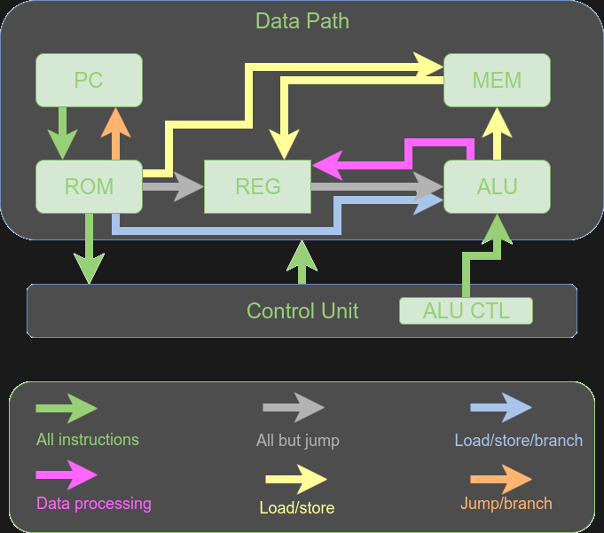
The processing occurs in an arithmetic logic unit (ALU) that performs different operations. The destination can be main memory or one of the registers. The register file uses an old trick to avoid a common problem. Suppose you can read one register per cycle. If you only allow one register in an instruction, that’s fine. But if you allow an instruction to do something like add two registers, you’ll have trouble loading both of them unless you stretch out the instruction time. That’s why the register file has two output ports.
The truth is, the register file is at least one spot where the design would not synthesize to real hardware as well as it could. For one thing, there’s a for loop in the initial block to zero the registers. Most synthesis tools would just throw that away. You’d be better off with a reset signal. The other possible issue depends on what exact FPGA you will target and what tools you use.
The designer provides two read ports to the registers, but the underlying storage is the same. This would make it difficult to use specialized RAM cells if they were available. Another common technique is to simply use two separate register blocks, one for each read port. A write will send data to both blocks so from the outside you can’t tell the difference. Frequently, though, this will result in a faster and more compact design.
It would be interesting (and not very difficult) to rewrite the register file to do this. However, if you aren’t going to build down to hardware you probably won’t notice any difference.
Like most similar CPUs, the whole control works out to muxes selecting what data gets sent where. In particular, there are four muxes in the processor’s data path:
- PCSrc – Routes the “next” PC value to the program counter
- RegDst – Selects what register to write from two fields in the instruction (the diagram shows three inputs, but that appears to be an error)
- BSrc – Selects the second argument to the ALU (either an immediate value or a register value)
- WBSrc – The “write back” mux selects what data is set back to the registers for writing
Design Tables
The rest of the design shows the thirteen instructions, the five instruction formats, and the control signals required for each of the formats. The nuances of the instructions in each category depend on what the ALU is set to do. In other words, an add instruction and a subtract instruction are exactly the same except for what the ALU does. As you might imagine, the ALU takes two inputs and an operation code and produces an output.
The original post doesn’t actually say which instructions are in which category, but it is pretty easy to puzzle out. The Load and Store instructions are in the memory access formats. The Branch on Equal and Not Equal instructions are in the branch category. The Jump instruction has its own format. All the other instructions are “data processing.” The one table shows a “hamming distance” op code, but this doesn’t appear anywhere else–including in the code–so I suspect it is a cut and paste error.
The two tables do a good job of summarizing the operations need to make the CPU work. There are nine distinct control signals:
- RegDst – This corresponds to the mux in the diagram of the same name and selects if the destination is a register (shows up as reg_dst in the code)
- ALUSrc – Selects the source of the ALU argument (same as the BSrc mux in the diagram, and shows up as alu_src in the code)
- MemtoReg – Active when a memory to register transfer occurs (mem_to_reg in the code)
- RegWrite – Set when write should go to a register (reg_write in the code)
- MemRead – Set when a memory read is the source data for the instruction (mem_read in the code)
- MemWrite – Set when memory is the write destination (mem_write in the code)
- Branch – Active when a branch is in progress (combination of beq and bne signals in the code)
- ALUOp – Combined with part of the instruction, selects the operation to perform in the ALU (alu_op in the code)
- Jump – Active when a jump is in progress
The table corresponds directly to Verilog in the control unit except for the name changes, which is unfortunate as it makes the table a little harder to follow. For example, here is the code for a data processing instruction with opcode 0010:
4'b0010: // data_processing
begin
  reg_dst = 1'b1;
  alu_src = 1'b0;
  mem_to_reg = 1'b0;
  reg_write = 1'b1;
  mem_read = 1'b0;
  mem_write = 1'b0;
  beq = 1'b0;
  bne = 1'b0;
  alu_op = 2'b00;
  jump = 1'b0;
end
Compare that to the table in the original post and you’ll see it maps directly. In English, the instruction is a read from two registers that writes back to the registers with an ALU operation code of 0 and it isn’t a jump or a branch.
Inexplicably, this block is duplicated for all the data processing instructions even though it shouldn’t be necessary. Luckily, for simulation, it won’t really matter and most synthesis tools will figure it out and merge the identical code for you.
Next Time
In the next installment, I’ll show you how to load the design into one of my favorite quick design tools, EDA Playground. There was a missing file and some massaging necessary to get it to work with the online tool. However, the CPU does work as promised, once you figure out a few peculiarities. If you want a sneak peek at the simulation, you can check out the video, below.


“For one thing, there’s a for loop in the initial block to zero the registers. Most synthesis tools would just throw that away. You’d be better off with a reset signal”
Modern synthesis tools for FPGAs have no problem with initial blocks to zero registers (of course, it won’t work on an ASIC). On the other hand, RAM doesn’t typically have a reset signal. Multiple read ports is no problem, and simply implemented by duplicating the RAM.
I haven’t tried it lately (mainly because I was taught not to do it), but I never put for loops in synthesizable code.
As for the dual port RAM that’s how I usually do it is to just have two copies (which is, of course, not area-friendly). I didn’t test to see if anything I synthesize with would pick that up from his code or not. I would bet against it, but I could be wrong and–of course–it would be dependent on the synthesizer.
For loops can be synthesized in the initial blocks. And a good synthesizer will automatically make multiple copies of the register file to support multiple read ports (or find another good implementation), so you don’t have to do it yourself.
On devices that support distributed RAM, dual read-port (or even triple) RAMs are much better for resources than regular registers.
I’ve used a lot of for loops in synthesized Verilog code. Some generate for loops and some other for loops that perform indexed opperations on a bit vector. I don’t know why everyone is afraid of for loops in Verilog RTL. Courses tend to teach you not to use for loops initially to avoid confusion early on but for loops exist in Verilog to make your life easier when applied properly and advanced users should look into using them.
I thought things like “for” were like a compiler directive and didn’t synthesis at all. Instead “for” modifies the HDL prior to synthesis so that the end result is achieved. The “for” is executed rather than synthesized.
I might be completely wrong though as I use VHDL rather than Verilog to avoid this exact ambiguity.
An asynchronous pre-set (or reset) state is different to initializing a state because it is achieved by using a bit from the configuration bit stream and XORing it with other logic to simply invert the logic block and that has the same effect as preset or reset. ie A pre-set block is simply a reset block that has an inverted output. However it is asynchronous and not in any way a synchronous loop so it would seem that synthesis has thrown it out if you believed that the “for” was some how synthesized.
Sure you can make a loop that initializes registers that *can* be synthesized but it would have to be synchronous (edge triggered for example) to some other clock or signal.
If there is no dependency on other signals then your probably writing a pre-synthesis (compiler) directive.
Hi Al,
I teach Verilog (and maintain EDA Playground). You absolutely can synthesise for loops. For for loops to be synthesisable, the loop bounds must be static. In other words, the maximum number of iterations must be fixed at compile time.
Matthew
Very interesting, looking forward to the follow-up. I use a feed for your articles now. https://feedly.com/i/subscription/feed/http://hackaday.com/author/wd5gnr1/feed/
Interesting. I have no experience with verilog or hdl. After you synthesize the code, how can you tell what is going to be programmed in the FPGA? In other words, if I compile code, I can do an objdump -d to see the result of the compilation including any optimizations. What is the equivalent in verilog? Is there a way to print an schematic of the synthesized code so that you can see what will end up programmed in the FPGA?
The actual “bitstream” (equivalent of machine code for a CPU) that you program into an FPGA doesn’t really have any “assembly language” representation that is (kind-of) human readable like objdump -d can show for a CPU executable. Most FPGAs use a proprietary bitstream format, but even the ones that have been reverse engineered generally just show “acres” of 1s and 0s that get programmed into LUTs, flip-flops and interconnections in the FPGA fabric (etc.).
However, most of the vendor toolchains have a “schematic level” diagram (or even lower level, showing FPGA primitives) that will make a (usually nested) graphical diagram of gates, LUTs, MUXes wires etc. However, for any medium size design, looking inside a given “component interface” (aka black box) the diagrams can easily become a “dense mess” (but still often handy to zoom in and “double check” that some HDL code turned into the hardware configuration you were expecting).
This why a lot of FPGA development is consists of simulation (so you can inspect the operation of a circuit in detail) and verification (unit tests etc. to verify correctness and that the tools did what you intended).
As Xark mentioned, there is usually a tool to view the implementation of your design included with the FPGA IDE (definitely true for both Altera and Xilinx), and at a minimum they spit out text summaries of ‘resource utilization’ with module-level breakdowns. FPGAs themselves are usually designed as a ‘sea of gates’ (typically a 4-6 input lookup table paired with a flip-flop as the minimum unit, with programmable routing resources connecting them together). When your verilog is ‘synthesized,’ it’s translated into combinations of LUTs and flip-flops (as well as other primitives like large block memories), and then it goes through a stage called ‘place and route’ (or sometimes ‘mapping’) where those LUTs and flip-flips are mapped onto the actual physical resources of the chip. In Xilinx’ Vivado tool, for instance, you can then pull up an ‘implementation view’ of the FPGA, which actually shows which LUTs and flip-flops are occupied, and if you click on the individual resources, you can see what logic signal it connects to. You can also do things like highlight all of the resources associated with a particular Verilog module, to get an idea of how your design was laid out. You pretty quickly get a good intuition for what the tool will do with your Verilog when you’re working closely with an FPGA.
I know the Xilinx HDL development environment (ISE) has a viewer so that you can see the schematic version of the code. You can even enter your code as a schematic. I would imagine that the Altera HDL development environment (Quartus) is the same but I have never gone looking for it.
The reality is that a modern FPGA will have a million or more gates so the schematic can end up huge and hard to navigate let alone understand.
Any help out there
I designed an 8051 uprocesor in verilog
In my decoder i had two long if else statements…and i am failing. Implementaion timing when i put defaults for the 4 decoder outputs
Any pointers
Can you post some code – the ‘if’ statements and the definition of those things that are tested for the ‘if’ conditionals.
my first attempt was
module Decoder(
input [7:0] OPC,//OP1,
output reg [1:0] OPC_length,
output reg [4:0] ALU_instruction,
output reg [4:0] Data_origin,
output reg [2:0] Data_dest
);
//////////////////////////////instruction function////////////////////////////////////
always @ (OPC)
begin
if (((OPC >= 8’h74) && (OPC = 8’h85) && (OPC = 8’hF5) && (OPC = 8’hE5) && (OPC = 8’hA6) && (OPC 8’h03) && (OPC 8’h13) && (OPC 8’h23) && (OPC 8’h33) && (OPC 8’h41) && (OPC 8’h51) && (OPC 8’h61) && (OPC 8’h93) && (OPC 8’hB3) && (OPC = 8’h38) && (OPC = 8’h48) && (OPC = 8’hC8) && (OPC = 8’h58) && (OPC = 8’h68) && (OPC = 8’h98) && (OPC = 8’h28) && (OPC = 8’hA6) && (OPC = 8’h08) && (OPC = 8’h18) && (OPC = 8’h88) && (OPC = 8’hE8) && (OPC = 8’hD8) && (OPC = 8’h74) && (OPC = 8’hB8) && (OPC = 8’hF5) && (OPC = 8’h23) && (OPC = 8’h33) && (OPC = 8’h44) && (OPC = 8’h54) && (OPC = 8’h64) && (OPC = 8’hC4) && (OPC = 8’h93) && (OPC = 8’hE2) && (OPC = 8’h08) && (OPC = 8’h18) && (OPC = 8’h78) && (OPC = 8’hA8) && (OPC = 8’hB8) && (OPC = 8’hD8) && (OPC = 8’hF8) && (OPC = 8’h85) && (OPC 3 bytes
Data_dest = 3’b011;//DIRECT
end
8’h86 : begin
OPC_length = 2’b10;
ALU_instruction = 5’b00001;
Data_origin = 5’b01001;//@RI ALONE
Data_dest = 3’b011;//DIRECT
end
8’h87 : begin
OPC_length = 2’b10;
ALU_instruction = 5’b00001;
Data_origin = 5’b01001;//@RI ALONE
Data_dest = 3’b011;//DIRECT
end
8’h88 : begin
OPC_length = 2’b10;
ALU_instruction = 5’b00001;
Data_origin = 5’b00110;//RB alone
Data_dest = 3’b011;//DIRECT
end
8’h89 : begin
OPC_length = 2’b10;
ALU_instruction = 5’b00001;
Data_origin = 5’b00110;//RB alone
Data_dest = 3’b011;//DIRECT
end
8’h8A : begin
OPC_length = 2’b10;
ALU_instruction = 5’b00001;
Data_origin = 5’b00110;//RB alone
Data_dest = 3’b011;//DIRECT
end
8’h8B : begin
OPC_length = 2’b10;
ALU_instruction = 5’b00001;
Data_origin = 5’b00110;//RB alone
Data_dest = 3’b011;//DIRECT
end
8’h8C : begin
OPC_length = 2’b10;
ALU_instruction = 5’b00001;
Data_origin = 5’b00110;//RB alone
Data_dest = 3’b011;//DIRECT
end
8’h8D : begin
OPC_length = 2’b10;
ALU_instruction = 5’b00001;
Data_origin = 5’b00110;//RB alone
Data_dest = 3’b011;//DIRECT
end
8’h8E : begin
OPC_length = 2’b10;
ALU_instruction = 5’b00001;
Data_origin = 5’b00110;//RB alone
Data_dest = 3’b011;//DIRECT
end
8’h8F : begin
OPC_length = 2’b10;
ALU_instruction = 5’b00001;
Data_origin = 5’b00110;//RB alone
Data_dest = 3’b011;//DIRECT
end
8’hF5 : begin
OPC_length = 2’b10;
ALU_instruction = 5’b00001;
Data_origin = 5’b10010;//acc alone for a move
Data_dest = 3’b011;//DIRECT
end
8’hF6 : begin
OPC_length = 2’b01;
ALU_instruction = 5’b00001;
Data_origin = 5’b10010;//acc alone for a move
Data_dest = 3’b010;//@RI
end
8’hF7 : begin
OPC_length = 2’b01;
ALU_instruction = 5’b00001;
Data_origin = 5’b10010;//acc alone for a move
Data_dest = 3’b010;//@RI
end
8’hF8 : begin
OPC_length = 2’b01;
ALU_instruction = 5’b00001;
Data_origin = 5’b10010;//acc alone for a move
Data_dest = 3’b001;//RB
end
8’hF9 : begin
OPC_length = 2’b01;
ALU_instruction = 5’b00001;
Data_origin = 5’b10010;//acc alone for a move
Data_dest = 3’b001;//RB
end
8’hFA : begin
OPC_length = 2’b01;
ALU_instruction = 5’b00001;
Data_origin = 5’b10010;//acc alone for a move
Data_dest = 3’b001;//RB
end
8’hFB : begin
OPC_length = 2’b01;
ALU_instruction = 5’b00001;
Data_origin = 5’b10010;//acc alone for a move
Data_dest = 3’b001;//RB
end
8’hFC : begin
OPC_length = 2’b01;
ALU_instruction = 5’b00001;
Data_origin = 5’b10010;//acc alone for a move
Data_dest = 3’b001;//RB
end
8’hFD : begin
OPC_length = 2’b01;
ALU_instruction = 5’b00001;
Data_origin = 5’b10010;//acc alone for a move
Data_dest = 3’b001;//RB
end
8’hFE : begin
OPC_length = 2’b01;
ALU_instruction = 5’b00001;
Data_origin = 5’b10010;//acc alone for a move
Data_dest = 3’b001;//RB
end
8’hFF : begin
OPC_length = 2’b01;
ALU_instruction = 5’b00001;
Data_origin = 5’b10010;//acc alone for a move
Data_dest = 3’b001;//RB
end
8’hE5 : begin
OPC_length = 2’b10;
ALU_instruction = 5’b00001;
Data_origin = 5’b00101;///DIRECT ALONE -> 2 bytes
Data_dest = 3’b000;// ACC
end
8’hE6 : begin
OPC_length = 2’b01;
ALU_instruction = 5’b00001;
Data_origin = 5’b01001;//@RI ALONE
Data_dest = 3’b000;// ACC
end
8’hE7 : begin
OPC_length = 2’b01;
ALU_instruction = 5’b00001;
Data_origin = 5’b01001;//@RI ALONE
Data_dest = 3’b000;// ACC
end
8’hE8 : begin
OPC_length = 2’b01;
ALU_instruction = 5’b00001;
Data_origin = 5’b00110;//RB alone
Data_dest = 3’b000;// ACC
end
8’hE9 : begin
OPC_length = 2’b01;
ALU_instruction = 5’b00001;
Data_origin = 5’b00110;//RB alone
Data_dest = 3’b000;// ACC
end
8’hEA : begin
OPC_length = 2’b01;
ALU_instruction = 5’b00001;
Data_origin = 5’b00110;//RB alone
Data_dest = 3’b000;// ACC
end
8’hEB : begin
OPC_length = 2’b01;
ALU_instruction = 5’b00001;
Data_origin = 5’b00110;//RB alone
Data_dest = 3’b000;// ACC
end
8’hEC : begin
OPC_length = 2’b01;
ALU_instruction = 5’b00001;
Data_origin = 5’b00110;//RB alone
Data_dest = 3’b000;// ACC
end
8’hED : begin
OPC_length = 2’b01;
ALU_instruction = 5’b00001;
Data_origin = 5’b00110;//RB alone
Data_dest = 3’b000;// ACC
end
8’hEE : begin
OPC_length = 2’b01;
ALU_instruction = 5’b00001;
Data_origin = 5’b00110;//RB alone
Data_dest = 3’b000;// ACC
end
8’hEF : begin
OPC_length = 2’b01;
ALU_instruction = 5’b00001;
Data_origin = 5’b00110;//RB alone
Data_dest = 3’b000;// ACC
end
8’hA6 : begin
OPC_length = 2’b01;
ALU_instruction = 5’b00001;
Data_origin = 5’b00101;///DIRECT ALONE -> 2 bytes
Data_dest = 3’b010;//@RI
end
8’hA7 : begin
OPC_length = 2’b01;
ALU_instruction = 5’b00001;
Data_origin = 5’b00101;///DIRECT ALONE -> 2 bytes
Data_dest = 3’b010;//@RI
end
8’hA8 : begin
OPC_length = 2’b01;
ALU_instruction = 5’b00001;
Data_origin = 5’b00101;///DIRECT ALONE -> 2 bytes
Data_dest = 3’b001;//RB
end
8’hA9 : begin
OPC_length = 2’b01;
ALU_instruction = 5’b00001;
Data_origin = 5’b00101;///DIRECT ALONE -> 2 bytes
Data_dest = 3’b001;//RB
end
8’hAA : begin
OPC_length = 2’b01;
ALU_instruction = 5’b00001;
Data_origin = 5’b00101;///DIRECT ALONE -> 2 bytes
Data_dest = 3’b001;//RB
end
8’hAB : begin
OPC_length = 2’b01;
ALU_instruction = 5’b00001;
Data_origin = 5’b00101;///DIRECT ALONE -> 2 bytes
Data_dest = 3’b001;//RB
end
8’hAC : begin
OPC_length = 2’b01;
ALU_instruction = 5’b00001;
Data_origin = 5’b00101;///DIRECT ALONE -> 2 bytes
Data_dest = 3’b001;//RB
end
8’hAD : begin
OPC_length = 2’b01;
ALU_instruction = 5’b00001;
Data_origin = 5’b00101;///DIRECT ALONE -> 2 bytes
Data_dest = 3’b001;//RB
end
8’hAE : begin
OPC_length = 2’b01;
ALU_instruction = 5’b00001;
Data_origin = 5’b00101;///DIRECT ALONE -> 2 bytes
Data_dest = 3’b001;//RB
end
8’hAF : begin
OPC_length = 2’b01;
ALU_instruction = 5’b00001;
Data_origin = 5’b00101;///DIRECT ALONE -> 2 bytes
Data_dest = 3’b001;//RB
end
8’hD0 : begin//pop
OPC_length = 2’b10;
ALU_instruction = 5’b00001;
Data_origin = 5’b01011; //stack
Data_dest = 3’b101;
end
8’hC0 : begin//push
OPC_length = 2’b10;
ALU_instruction = 5’b00001;
Data_origin = 5’b01010;
Data_dest = 3’b100;//stack
end
/////////////////////////END OF MOV///////////////////////////
8’h03 : begin
OPC_length = 2’b01;
ALU_instruction = 5’b01101;
Data_origin = 5’b01000;//ACC alone
Data_dest = 3’b000;// ACC
end
///////////////////////// RR ////////////////////////////
8’h04 : begin
OPC_length = 2’b01;
ALU_instruction = 5’b00010;
Data_origin = 5’b01000;//ACC alone
Data_dest = 3’b000;// ACC
end
8’h05 : begin
OPC_length = 2’b10;
ALU_instruction = 5’b00010;
Data_origin = 5’b00101;///DIRECT ALONE -> 2 bytes
Data_dest = 3’b011;//DIRECT
end
8’h06 : begin
OPC_length = 2’b01;
ALU_instruction = 5’b00010;
Data_origin = 5’b01001;//@RI ALONE
Data_dest = 3’b010;//@RI
end
8’h07 : begin
OPC_length = 2’b01;
ALU_instruction = 5’b00010;
Data_origin = 5’b01001;//@RI ALONE
Data_dest = 3’b010;//@RI
end
8’h08 : begin
OPC_length = 2’b01;
ALU_instruction = 5’b00010;
Data_origin = 5’b00110;//RB alone
Data_dest = 3’b001;//RB
end
8’h09 : begin
OPC_length = 2’b01;
ALU_instruction = 5’b00010;
Data_origin = 5’b00110;//RB alone
Data_dest = 3’b001;//RB
end
8’h0A : begin
OPC_length = 2’b01;
ALU_instruction = 5’b00010;
Data_origin = 5’b00110;//RB alone
Data_dest = 3’b001;//RB
end
8’h0B : begin
OPC_length = 2’b01;
ALU_instruction = 5’b00010;
Data_origin = 5’b00110;//RB alone
Data_dest = 3’b001;//RB
end
8’h0C : begin
OPC_length = 2’b01;
ALU_instruction = 5’b00010;
Data_origin = 5’b00110;//RB alone
Data_dest = 3’b001;//RB
end
8’h0D : begin
OPC_length = 2’b01;
ALU_instruction = 5’b00010;
Data_origin = 5’b00110;//RB alone
Data_dest = 3’b001;//RB
end
8’h0E : begin
OPC_length = 2’b01;
ALU_instruction = 5’b00010;
Data_origin = 5’b00110;//RB alone
Data_dest = 3’b001;//RB
end
8’h0F : begin
OPC_length = 2’b01;
ALU_instruction = 5’b00010;
Data_origin = 5’b00110;//RB alone
Data_dest = 3’b001;//RB
end
///////////////////////// END OF INC /////////////////////////
8’h13 : begin
OPC_length = 2’b01;
ALU_instruction = 5’b01111;
Data_origin = 5’b01000;//ACC alone
Data_dest = 3’b000;// ACC
end
///////////////////////// END OF RRC ////////////////////////
8’h14 : begin
OPC_length = 2’b01;
ALU_instruction = 5’b00011;
Data_origin = 5’b01000;//ACC alone
Data_dest = 3’b000;// ACC
end
8’h15 : begin
OPC_length = 2’b10;
ALU_instruction = 5’b00011;
Data_origin = 5’b00101;///DIRECT ALONE -> 2 bytes
Data_dest = 3’b011;//DIRECT
end
8’h16 : begin
OPC_length = 2’b01;
ALU_instruction = 5’b00011;
Data_origin = 5’b01001;//@RI ALONE
Data_dest = 3’b010;//@RI
end
8’h17 : begin
OPC_length = 2’b01;
ALU_instruction = 5’b00011;
Data_origin = 5’b01001;//@RI ALONE
Data_dest = 3’b010;//@RI
end
8’h18 : begin
OPC_length = 2’b01;
ALU_instruction = 5’b00011;
Data_origin = 5’b00110;//RB alone
Data_dest = 3’b001;//RB
end
8’h19 : begin
OPC_length = 2’b01;
ALU_instruction = 5’b00011;
Data_origin = 5’b00110;//RB alone
Data_dest = 3’b001;//RB
end
8’h1A : begin
OPC_length = 2’b01;
ALU_instruction = 5’b00011;
Data_origin = 5’b00110;//RB alone
Data_dest = 3’b001;//RB
end
8’h1B : begin
OPC_length = 2’b01;
ALU_instruction = 5’b00011;
Data_origin = 5’b00110;//RB alone
Data_dest = 3’b001;//RB
end
8’h1C : begin
OPC_length = 2’b01;
ALU_instruction = 5’b00011;
Data_origin = 5’b00110;//RB alone
Data_dest = 3’b001;//RB
end
8’h1D : begin
OPC_length = 2’b01;
ALU_instruction = 5’b00011;
Data_origin = 5’b00110;//RB alone
Data_dest = 3’b001;//RB
end
8’h1E : begin
OPC_length = 2’b01;
ALU_instruction = 5’b00011;
Data_origin = 5’b00110;//RB alone
Data_dest = 3’b001;//RB
end
8’h1F : begin
OPC_length = 2’b01;
ALU_instruction = 5’b00011;
Data_origin = 5’b00110;//RB alone
Data_dest = 3’b001;//RB
end
///////////////////////// END OF DEC //////////////////////////
8’h23 : begin
OPC_length = 2’b01;
ALU_instruction = 5’b01110;
Data_origin = 5’b01000;//ACC alone
Data_dest = 3’b000;// ACC
end
///////////////////////// RL ///////////////////////////////////
8’h24 : begin
OPC_length = 2’b10;
ALU_instruction = 5’b00100;
Data_origin = 5’b00000;//ACC(SFR) & IMMEDIATE
Data_dest = 3’b000;// ACC
end
8’h25 : begin
OPC_length = 2’b10;
ALU_instruction = 5’b00100;
Data_origin = 5’b00010;//from ACC & DIRECT
Data_dest = 3’b000;// ACC
end
8’h26 : begin
OPC_length = 2’b01;
ALU_instruction = 5’b00100;
Data_origin = 5’b00011;//from ACC & @Ri
Data_dest = 3’b000;// ACC
end
8’h27 : begin
OPC_length = 2’b01;
ALU_instruction = 5’b00100;
Data_origin = 5’b00011;//from ACC & @Ri
Data_dest = 3’b000;// ACC
end
8’h28 : begin
OPC_length = 2’b01;
ALU_instruction = 5’b00100;
Data_origin = 5’b00001;//ACC(SFR) & RB
Data_dest = 3’b000;// ACC
end
8’h29 : begin
OPC_length = 2’b01;
ALU_instruction = 5’b00100;
Data_origin = 5’b00001;//ACC(SFR) & RB
Data_dest = 3’b000;// ACC
end
8’h2A : begin
OPC_length = 2’b01;
ALU_instruction = 5’b00100;
Data_origin = 5’b00001;//ACC(SFR) & RB
Data_dest = 3’b000;// ACC
end
8’h2B : begin
OPC_length = 2’b01;
ALU_instruction = 5’b00100;
Data_origin = 5’b00001;//ACC(SFR) & RB
Data_dest = 3’b000;// ACC
end
8’h2C : begin
OPC_length = 2’b01;
ALU_instruction = 5’b00100;
Data_origin = 5’b00001;//ACC(SFR) & RB
Data_dest = 3’b000;// ACC
end
8’h2D : begin
OPC_length = 2’b01;
ALU_instruction = 5’b00100;
Data_origin = 5’b00001;//ACC(SFR) & RB
Data_dest = 3’b000;// ACC
end
8’h2E : begin
OPC_length = 2’b01;
ALU_instruction = 5’b00100;
Data_origin = 5’b00001;//ACC(SFR) & RB
Data_dest = 3’b000;// ACC
end
8’h2F : begin
OPC_length = 2’b01;
ALU_instruction = 5’b00100;
Data_origin = 5’b00001;//ACC(SFR) & RB
Data_dest = 3’b000;// ACC
end
///////////////////////// END OF ADD A ///////////////////////////////////
8’h33 : begin
OPC_length = 2’b01;
ALU_instruction = 5’b10000;
Data_origin = 5’b01000;//ACC alone
Data_dest = 3’b000;// ACC
end
///////////////////////// END OF RLC ///////////////////////////////////
8’h34 : begin
OPC_length = 2’b10;
ALU_instruction = 5’b00101;
Data_origin = 5’b00000;//ACC(SFR) & IMMEDIATE
Data_dest = 3’b000;// ACC
end
8’h35 : begin
OPC_length = 2’b10;
ALU_instruction = 5’b00101;
Data_origin = 5’b00010;//from ACC & DIRECT
Data_dest = 3’b000;// ACC
end
8’h36 : begin
OPC_length = 2’b01;
ALU_instruction = 5’b00101;
Data_origin = 5’b00011;//from ACC & @Ri
Data_dest = 3’b000;// ACC
end
8’h37 : begin
OPC_length = 2’b01;
ALU_instruction = 5’b00101;
Data_origin = 5’b00011;//from ACC & @Ri
Data_dest = 3’b000;// ACC
end
8’h38 : begin
OPC_length = 2’b01;
ALU_instruction = 5’b00101;
Data_origin = 5’b00001;//ACC(SFR) & RB
Data_dest = 3’b000;// ACC
end
8’h39 : begin
OPC_length = 2’b01;
ALU_instruction = 5’b00101;
Data_origin = 5’b00001;//ACC(SFR) & RB
Data_dest = 3’b000;// ACC
end
8’h3A : begin
OPC_length = 2’b01;
ALU_instruction = 5’b00101;
Data_origin = 5’b00001;//ACC(SFR) & RB
Data_dest = 3’b000;// ACC
end
8’h3B : begin
OPC_length = 2’b01;
ALU_instruction = 5’b00101;
Data_origin = 5’b00001;//ACC(SFR) & RB
Data_dest = 3’b000;// ACC
end
8’h3C : begin
OPC_length = 2’b01;
ALU_instruction = 5’b00101;
Data_origin = 5’b00001;//ACC(SFR) & RB
Data_dest = 3’b000;// ACC
end
8’h3D : begin
OPC_length = 2’b01;
ALU_instruction = 5’b00101;
Data_origin = 5’b00001;//ACC(SFR) & RB
Data_dest = 3’b000;// ACC
end
8’h3E : begin
OPC_length = 2’b01;
ALU_instruction = 5’b00101;
Data_origin = 5’b00001;//ACC(SFR) & RB
Data_dest = 3’b000;// ACC
end
8’h3F : begin
OPC_length = 2’b01;
ALU_instruction = 5’b00101;
Data_origin = 5’b00001;//ACC(SFR) & RB
Data_dest = 3’b000;// ACC
end
///////////////////////// END OF ADDC A ///////////////////////////////////
8’h42 : begin
OPC_length = 2’b10;
ALU_instruction = 5’b00110;
Data_origin = 5’b00010;//from ACC & DIRECT
Data_dest = 3’b011;//DIRECT
end
8’h43 : begin
OPC_length = 2’b11;
ALU_instruction = 5’b00110;
Data_origin = 5’b00100;//direct and IMMEDIATE
Data_dest = 3’b011;//DIRECT
end
8’h44 : begin
OPC_length = 2’b10;
ALU_instruction = 5’b00110;
Data_origin = 5’b00000;//ACC(SFR) & IMMEDIATE
Data_dest = 3’b000;// ACC
end
8’h45 : begin
OPC_length = 2’b10;
ALU_instruction = 5’b00110;
Data_origin = 5’b00010;//from ACC & DIRECT
Data_dest = 3’b000;// ACC
end
8’h46 : begin
OPC_length = 2’b01;
ALU_instruction = 5’b00110;
Data_origin = 5’b00011;//from ACC & @Ri
Data_dest = 3’b000;// ACC
end
8’h47 : begin
OPC_length = 2’b01;
ALU_instruction = 5’b00110;
Data_origin = 5’b00011;//from ACC & @Ri
Data_dest = 3’b000;// ACC
end
8’h48 : begin
OPC_length = 2’b01;
ALU_instruction = 5’b00110;
Data_origin = 5’b00001;//ACC(SFR) & RB
Data_dest = 3’b000;// ACC
end
8’h49 : begin
OPC_length = 2’b01;
ALU_instruction = 5’b00110;
Data_origin = 5’b00001;//ACC(SFR) & RB
Data_dest = 3’b000;// ACC
end
8’h4A : begin
OPC_length = 2’b01;
ALU_instruction = 5’b00110;
Data_origin = 5’b00001;//ACC(SFR) & RB
Data_dest = 3’b000;// ACC
end
8’h4B : begin
OPC_length = 2’b01;
ALU_instruction = 5’b00110;
Data_origin = 5’b00001;//ACC(SFR) & RB
Data_dest = 3’b000;// ACC
end
8’h4C : begin
OPC_length = 2’b01;
ALU_instruction = 5’b00110;
Data_origin = 5’b00001;//ACC(SFR) & RB
Data_dest = 3’b000;// ACC
end
8’h4D : begin
OPC_length = 2’b01;
ALU_instruction = 5’b00110;
Data_origin = 5’b00001;//ACC(SFR) & RB
Data_dest = 3’b000;// ACC
end
8’h4E : begin
OPC_length = 2’b01;
ALU_instruction = 5’b00110;
Data_origin = 5’b00001;//ACC(SFR) & RB
Data_dest = 3’b000;// ACC
end
8’h4F : begin
OPC_length = 2’b01;
ALU_instruction = 5’b00110;
Data_origin = 5’b00001;//ACC(SFR) & RB
Data_dest = 3’b000;// ACC
end
///////////////////// END OF ORL A //////////////////////////////
8’h52 : begin
OPC_length = 2’b10;
ALU_instruction = 5’b00111;
Data_origin = 5’b00010;//from ACC & DIRECT
Data_dest = 3’b011;//DIRECT
end
8’h53 : begin
OPC_length = 2’b11;
ALU_instruction = 5’b00111;
Data_origin = 5’b00100;//direct and IMMEDIATE
Data_dest = 3’b011;//DIRECT
end
8’h54 : begin
OPC_length = 2’b10;
ALU_instruction = 5’b00111;
Data_origin = 5’b00000;//ACC(SFR) & IMMEDIATE
Data_dest = 3’b000;// ACC
end
8’h55 : begin
OPC_length = 2’b10;
ALU_instruction = 5’b00111;
Data_origin = 5’b00010;//from ACC & DIRECT
Data_dest = 3’b000;// ACC
end
8’h56 : begin
OPC_length = 2’b01;
ALU_instruction = 5’b00111;
Data_origin = 5’b00011;//from ACC & @Ri
Data_dest = 3’b000;// ACC
end
8’h57 : begin
OPC_length = 2’b01;
ALU_instruction = 5’b00111;
Data_origin = 5’b00011;//from ACC & @Ri
Data_dest = 3’b000;// ACC
end
8’h58 : begin
OPC_length = 2’b01;
ALU_instruction = 5’b00111;
Data_origin = 5’b00001;//ACC(SFR) & RB
Data_dest = 3’b000;// ACC
end
8’h59 : begin
OPC_length = 2’b01;
ALU_instruction = 5’b00111;
Data_origin = 5’b00001;//ACC(SFR) & RB
Data_dest = 3’b000;// ACC
end
8’h5A : begin
OPC_length = 2’b01;
ALU_instruction = 5’b00111;
Data_origin = 5’b00001;//ACC(SFR) & RB
Data_dest = 3’b000;// ACC
end
8’h5B : begin
OPC_length = 2’b01;
ALU_instruction = 5’b00111;
Data_origin = 5’b00001;//ACC(SFR) & RB
Data_dest = 3’b000;// ACC
end
8’h5C : begin
OPC_length = 2’b01;
ALU_instruction = 5’b00111;
Data_origin = 5’b00001;//ACC(SFR) & RB
Data_dest = 3’b000;// ACC
end
8’h5D : begin
OPC_length = 2’b01;
ALU_instruction = 5’b00111;
Data_origin = 5’b00001;//ACC(SFR) & RB
Data_dest = 3’b000;// ACC
end
8’h5E : begin
OPC_length = 2’b01;
ALU_instruction = 5’b00111;
Data_origin = 5’b00001;//ACC(SFR) & RB
Data_dest = 3’b000;// ACC
end
8’h5F : begin
OPC_length = 2’b01;
ALU_instruction = 5’b00111;
Data_origin = 5’b00001;//ACC(SFR) & RB
Data_dest = 3’b000;// ACC
end
///////////////////// END OF ANL A //////////////////////////////
8’h62 : begin
OPC_length = 2’b10;
ALU_instruction = 5’b01000;
Data_origin = 5’b00010;//from ACC & DIRECT
Data_dest = 3’b011;//DIRECT
end
8’h63 : begin
OPC_length = 2’b11;
ALU_instruction = 5’b01000;
Data_origin = 5’b00100;//direct and IMMEDIATE
Data_dest = 3’b011;//DIRECT
end
8’h64 : begin
OPC_length = 2’b10;
ALU_instruction = 5’b01000;
Data_origin = 5’b00000;//ACC(SFR) & IMMEDIATE
Data_dest = 3’b000;// ACC
end
8’h65 : begin
OPC_length = 2’b10;
ALU_instruction = 5’b01000;
Data_origin = 5’b00010;//from ACC & DIRECT
Data_dest = 3’b000;// ACC
end
8’h66 : begin
OPC_length = 2’b01;
ALU_instruction = 5’b01000;
Data_origin = 5’b00011;//from ACC & @Ri
Data_dest = 3’b000;// ACC
end
8’h67 : begin
OPC_length = 2’b01;
ALU_instruction = 5’b01000;
Data_origin = 5’b00011;//from ACC & @Ri
Data_dest = 3’b000;// ACC
end
8’h68 : begin
OPC_length = 2’b01;
ALU_instruction = 5’b01000;
Data_origin = 5’b00001;//ACC(SFR) & RB
Data_dest = 3’b000;// ACC
end
8’h69 : begin
OPC_length = 2’b01;
ALU_instruction = 5’b01000;
Data_origin = 5’b00001;//ACC(SFR) & RB
Data_dest = 3’b000;// ACC
end
8’h6A : begin
OPC_length = 2’b01;
ALU_instruction = 5’b01000;
Data_origin = 5’b00001;//ACC(SFR) & RB
Data_dest = 3’b000;// ACC
end
8’h6B : begin
OPC_length = 2’b01;
ALU_instruction = 5’b01000;
Data_origin = 5’b00001;//ACC(SFR) & RB
Data_dest = 3’b000;// ACC
end
8’h6C : begin
OPC_length = 2’b01;
ALU_instruction = 5’b01000;
Data_origin = 5’b00001;//ACC(SFR) & RB
Data_dest = 3’b000;// ACC
end
8’h6D : begin
OPC_length = 2’b01;
ALU_instruction = 5’b01000;
Data_origin = 5’b00001;//ACC(SFR) & RB
Data_dest = 3’b000;// ACC
end
8’h6E : begin
OPC_length = 2’b01;
ALU_instruction = 5’b01000;
Data_origin = 5’b00001;//ACC(SFR) & RB
Data_dest = 3’b000;// ACC
end
8’h6F : begin
OPC_length = 2’b01;
ALU_instruction = 5’b01000;
Data_origin = 5’b00001;//ACC(SFR) & RB
Data_dest = 3’b000;// ACC
end
///////////////////// END OF XRL A //////////////////////////////
8’h94 : begin
OPC_length = 2’b10;
ALU_instruction = 5’b01001;
Data_origin = 5’b00000;//ACC(SFR) & IMMEDIATE
Data_dest = 3’b000;// ACC
end
8’h95 : begin
OPC_length = 2’b10;
ALU_instruction = 5’b01001;
Data_origin = 5’b00010;//from ACC & DIRECT
Data_dest = 3’b000;// ACC
end
8’h96 : begin
OPC_length = 2’b01;
ALU_instruction = 5’b01001;
Data_origin = 5’b00011;//from ACC & @Ri
Data_dest = 3’b000;// ACC
end
8’h97 : begin
OPC_length = 2’b01;
ALU_instruction = 5’b01001;
Data_origin = 5’b00011;//from ACC & @Ri
Data_dest = 3’b000;// ACC
end
8’h98 : begin
OPC_length = 2’b01;
ALU_instruction = 5’b01001;
Data_origin = 5’b00001;//ACC(SFR) & RB
Data_dest = 3’b000;// ACC
end
8’h99 : begin
OPC_length = 2’b01;
ALU_instruction = 5’b01001;
Data_origin = 5’b00001;//ACC(SFR) & RB
Data_dest = 3’b000;// ACC
end
8’h9A : begin
OPC_length = 2’b01;
ALU_instruction = 5’b01001;
Data_origin = 5’b00001;//ACC(SFR) & RB
Data_dest = 3’b000;// ACC
end
8’h9B : begin
OPC_length = 2’b01;
ALU_instruction = 5’b01001;
Data_origin = 5’b00001;//ACC(SFR) & RB
Data_dest = 3’b000;// ACC
end
8’h9C : begin
OPC_length = 2’b01;
ALU_instruction = 5’b01001;
Data_origin = 5’b00001;//ACC(SFR) & RB
Data_dest = 3’b000;// ACC
end
8’h9D : begin
OPC_length = 2’b01;
ALU_instruction = 5’b01001;
Data_origin = 5’b00001;//ACC(SFR) & RB
Data_dest = 3’b000;// ACC
end
8’h9E : begin
OPC_length = 2’b01;
ALU_instruction = 5’b01001;
Data_origin = 5’b00001;//ACC(SFR) & RB
Data_dest = 3’b000;// ACC
end
8’h9F : begin
OPC_length = 2’b01;
ALU_instruction = 5’b01001;
Data_origin = 5’b00001;//ACC(SFR) & RB
Data_dest = 3’b000;// ACC
end
///////////////////// END OF SUBB A //////////////////////////////
8’hB4 : begin
OPC_length = 2’b11;
ALU_instruction = 5’b01100;
Data_origin = 5’b00000;//ACC(SFR) & IMMEDIATE
end
8’hB5 : begin
OPC_length = 2’b11;
ALU_instruction = 5’b01100;
Data_origin = 5’b00010;//from ACC & DIRECT
end
8’hB6 : begin
OPC_length = 2’b11;
ALU_instruction = 5’b01100;
Data_origin = 5’b10001;//@ri & immed
end
8’hB7 : begin
OPC_length = 2’b11;
ALU_instruction = 5’b01100;
Data_origin = 5’b10001;//@ri & immed
end
8’hB8 : begin
OPC_length = 2’b11;
ALU_instruction = 5’b01100;
Data_origin = 5’b01100; //register bank and immediate
end
8’hB9 : begin
OPC_length = 2’b11;
ALU_instruction = 5’b01100;
Data_origin = 5’b01100; //register bank and immediate
end
8’hBA : begin
OPC_length = 2’b11;
ALU_instruction = 5’b01100;
Data_origin = 5’b01100; //register bank and immediate
end
8’hBB : begin
OPC_length = 2’b11;
ALU_instruction = 5’b01100;
Data_origin = 5’b01100; //register bank and immediate
end
8’hBC : begin
OPC_length = 2’b11;
ALU_instruction = 5’b01100;
Data_origin = 5’b01100; //register bank and immediate
end
8’hBD : begin
OPC_length = 2’b11;
ALU_instruction = 5’b01100;
Data_origin = 5’b01100; //register bank and immediate
end
8’hBE : begin
OPC_length = 2’b11;
ALU_instruction = 5’b01100;
Data_origin = 5’b01100; //register bank and immediate
end
8’hBF : begin
OPC_length = 2’b11;
ALU_instruction = 5’b01100;
Data_origin = 5’b01100; //register bank and immediate
end
///////////////////// END OF CJNE //////////////////////////////
8’hD5 : begin
OPC_length = 2’b11;
ALU_instruction = 5’b10010;
Data_origin = 5’b00101;///DIRECT ALONE -> 2 bytes
Data_dest = 3’b011;//DIRECT
end
8’hD8 : begin
OPC_length = 2’b10;
ALU_instruction = 5’b10010;
Data_origin = 5’b00110;//RB alone
Data_dest = 3’b001;//RB
end
8’hD9 : begin
OPC_length = 2’b10;
ALU_instruction = 5’b10010;
Data_origin = 5’b00110;//RB alone
Data_dest = 3’b001;//RB
end
8’hDA : begin
OPC_length = 2’b10;
ALU_instruction = 5’b10010;
Data_origin = 5’b00110;//RB alone
Data_dest = 3’b001;//RB
end
8’hDB : begin
OPC_length = 2’b10;
ALU_instruction = 5’b10010;
Data_origin = 5’b00110;//RB alone
Data_dest = 3’b001;//RB
end
8’hDC : begin
OPC_length = 2’b10;
ALU_instruction = 5’b10010;
Data_origin = 5’b00110;//RB alone
Data_dest = 3’b001;//RB
end
8’hDD : begin
OPC_length = 2’b10;
ALU_instruction = 5’b10010;
Data_origin = 5’b00110;//RB alone
Data_dest = 3’b001;//RB
end
8’hDE : begin
OPC_length = 2’b10;
ALU_instruction = 5’b10010;
Data_origin = 5’b00110;//RB alone
Data_dest = 3’b001;//RB
end
8’hDF : begin
OPC_length = 2’b10;
ALU_instruction = 5’b10010;
Data_origin = 5’b00110;//RB alone
Data_dest = 3’b001;//RB
end
///////////////////// END OF DJNZ //////////////////////////////
8’h40 : begin//JC
OPC_length = 2’b10;
Data_origin = 5’b10111;
end
//////////////////////////////////////////////////////////////
8’h50 : begin//JNC
OPC_length = 2’b10;
Data_origin = 5’b10100;
end
//////////////////////////////////////////////////////////////
8’h70 : begin//JNZ
OPC_length = 2’b10;
Data_origin = 5’b10110;
end
//////////////////////////////////////////////////////////////
8’h60 : begin//JZ
OPC_length = 2’b10;
Data_origin = 5’b10101;
end
//////////////////////////////////////////////////////////////
8’h02 : begin//LJUMP
OPC_length = 2’b11;
Data_origin = 5’b01101;
end
///////////////////////////////////////////////////////////////
8’h80 : begin//SJUMP
OPC_length = 2’b10;
Data_origin = 5’b10000;
end
//////////////////////////////////////////////////////////////
8’hD3 : begin//set CARRY
OPC_length = 2’b01;
Data_origin = 5’b01110;
end
//////////////////////////////////////////////////////////////
8’hE4 : begin// CLR A
OPC_length = 2’b01;
Data_origin = 5’b11000;
end
//////////////////////////////////////////////////////////////
8’h00 : begin// NOP
OPC_length = 2’b01;
Data_origin = 5’b11001;
end
//////////////////////////////////////////////////////////////
endcase
end
endmodule
i still cant find a way to default so i decided to use 4 always blocks for default, that way since i have an fsm controlling the executing part, and controlling signalls i can default for example ALU_instruction to a move, which wont affect the code, or rather shouldnt not because instructions that dont need the ALU for execution are are executed in state 1 of my fsm
module efsm(
/////////////////// inputs /////////////////////////////
input clk,
input reset,
input RAM_SFR_sel,
input cy_bit,
input [7:0] ACC,
input fetch_complete,
input [4:0] Data_origin,
input [2:0] Data_dest,
input comp_s_jump,
input comp_l_jump,
////////////////// outputs ////////////////////////////
output reg [7:0] SFR_sel,
output reg RAM_wr,
output reg SFR_wr,
output reg dec_SP,
output reg inc_SP,
output reg load_PC,
output reg [1:0] load_PC_sel,
output reg [1:0] A_In_Sel,
output reg [1:0] B_In_Sel,
output reg enable_PSW,
output reg enable_ACC,
output reg enable_RAM,
output reg execute_complete,
output reg execute_complete_led,
output reg set_B,
output reg clr_ACC,
output reg [2:0] Add_Gen_Sel
);
///////////////// states ///////////////////////////////
reg [2:0] e_nState;
reg [2:0] e_pState;
parameter s0 = 3’b000;//0
parameter s1 = 3’b001;//1
parameter s2 = 3’b010;//2
parameter s3 = 3’b011;//3
parameter s4 = 3’b100;//4
parameter s5 = 3’b101;//5
////////////////////////////////////fun begins////////////
always@(posedge clk)
begin//sync_process
if(reset)
e_pState <= s0;
else
e_pState 2 bytes
Add_Gen_Sel = 3’b000;//select op1
enable_RAM = 1’b1;
end
5’b10011:begin//direct alone -> 3 bytes
Add_Gen_Sel = 3’b001;//select op2
enable_RAM = 1’b1;
end
5’b00110:begin//RB
Add_Gen_Sel = 3’b010;//select op1
enable_RAM = 1’b1;
end
5’b01001:begin//@ri
Add_Gen_Sel = 3’b100;//ram data
enable_RAM = 1’b1;
end
5’b00011:begin//acc & @ri
SFR_sel = 8’hE0;//sel ACC in SFR mux
Add_Gen_Sel = 3’b100;//ram data
enable_RAM = 1’b1;
end
5’b01010:begin//push
Add_Gen_Sel = 3’b000;//op1
enable_RAM = 1’b1;
end
5’b01011:begin//pop
Add_Gen_Sel = 3’b101;//stack pointer
enable_RAM = 1’b1;
dec_SP = 1’b1;
end
5’b01100:begin//rb and immed
Add_Gen_Sel = 3’b010;
enable_RAM = 1’b1;
end
5’b10001:begin//@ri & immed
Add_Gen_Sel = 3’b100;//rom data
enable_RAM = 1’b1;
end
///////////default ->////////////////
// default: Add_Gen_Sel = 3’b111;//default
endcase
e_nState = s3;
end
/////////////////////// select muxes///////////////////////////////////
s3:begin
case(Data_origin)
5’b00000:begin //ACC & #IMMEDIATE
A_In_Sel = 2’b00;//from acc -> sfr
B_In_Sel = 2’b01;//from op1
end
5’b00001:begin//acc & rb
A_In_Sel = 2’b00;//from acc -> sfr
B_In_Sel = 2’b11;//from ram
end
5’b00010:begin//acc & direct
A_In_Sel = 2’b00;//from acc -> sfr
B_In_Sel = 2’b11;//from ram
end
5’b00011:begin//acc & @ri
A_In_Sel = 2’b00;//from acc -> sfr
B_In_Sel = 2’b11;//from ram
end
5’b00100:begin//direct and immediate
A_In_Sel = 2’b10;//from ram
B_In_Sel = 2’b10;//from op2
end
5’b00101:begin///direct
B_In_Sel = 2’b11;//from ram
end
5’b00110:begin//rb
B_In_Sel = 2’b11;//from ram
end
5’b00111:begin//immediate
B_In_Sel = 2’b01;//from op1
end
5’b01000:begin//acc
A_In_Sel = 2’b00;//from acc -> sfr
end
5’b10010:begin//acc for move
B_In_Sel = 2’b00;//from acc -> sfr
end
5’b01001:begin//@ri
B_In_Sel = 2’b11;//from ram
end
5’b01010:begin//push
B_In_Sel = 2’b11;//from ram
end
5’b01011:begin//pop
B_In_Sel = 2’b11;//from ram
end
5’b01100:begin//cjne
A_In_Sel = 2’b10;//from ram
B_In_Sel = 2’b01;//from op1
end
5’b10001:begin//@ri & immed
A_In_Sel = 2’b10;//from ram
B_In_Sel = 2’b01;//from op1
end
endcase
//////////////////////////////////////comparison execution////////////////
if(comp_s_jump)//in 2 byte instructions
begin
load_PC_sel = 2’b00;
load_PC = 1’b1;
e_nState = s5;
end
if(comp_l_jump)//in 3 byte instructions
begin
load_PC_sel = 2’b10;
load_PC = 1’b1;
e_nState = s5;
end
//////////////////////////////////////data destination////////////////////////
case(Data_dest)
3’b000:begin//acc
enable_ACC = 1’b1;
SFR_wr = 1’b1;
e_nState = s5;
end
3’b001:begin//register banks
Add_Gen_Sel = 3’b010;
RAM_wr = 1’b1;
enable_RAM = 1’b1;
e_nState = s5;
end
3’b011:begin//DIRECT BYTE
Add_Gen_Sel = 3’b000;
if(RAM_SFR_sel)
SFR_wr = 1’b1;
else
begin
RAM_wr = 1’b1;
enable_RAM = 1’b1;
end
e_nState = s5;
end
3’b010:begin//@ri
Add_Gen_Sel = 3’b011;
RAM_wr = 1’b1;
enable_RAM = 1’b1;
e_nState = s4;
end
3’b100:begin///pushing
Add_Gen_Sel = 3’b101;//from sp
RAM_wr = 1’b1;
enable_RAM = 1’b1;
e_nState = s5;
end
3’b101:begin//popping
Add_Gen_Sel = 3’b000;//from op1
RAM_wr = 1’b1;
enable_RAM = 1’b1;
e_nState = s5;
end
3’b110:begin//set_B
enable_PSW = 1’b1;
e_nState = s5;
end
endcase
end//s3
/////////////////////////////////////////////////////////////////////////////
s4:begin
Add_Gen_Sel = 3’b100;//indirect ram
RAM_wr = 1’b1;
enable_RAM = 1’b1;
e_nState = s5;
end
s5:begin
execute_complete = 1’b1;
execute_complete_led = 1’b1;
e_nState = s0;
end
default:e_nState = s0;
endcase
end
endmodule
I do VHDL so perhaps some else can help as well.
Firstly
always @ (OPC)

begin

if (((OPC >= 8’h74) && (OPC = 8’h85) ... && (OPC 3 bytes

Data_dest = 3’b011;//DIRECT

end
The IF should always be true because your using assignment rather than a comparitor. There are also missing brackets but I suspect that is from wordpress limiting line length.
Perhaps you meant (‘==’ instead of ‘=’) –
always @ (OPC)

begin

if (((OPC >= 8’h74) && (OPC == 8’h85) ... && (OPC 3 bytes

Data_dest = 3’b011;//DIRECT

end
Or perhaps even this (one bracket shifted to the second part of ‘if’ and all but first Boolean changed to OR –
always @ (OPC)

begin

if ((OPC >= 8’h74) && ((OPC == 8’h85) ... || (OPC 3 bytes

Data_dest = 3’b011;//DIRECT

end
The rest looks like a switch / case or whatever is the equivalent in Verilog and that part looks ok. It’s just missing the switch at the beginning and that was probably eaten by wordpress to.
You could probably just drop the “if” altogether and add a “default” case. If Verilog optimizes like VHDL then these two things would end up the same anyway.
http://www.fpga4student.com/2017/04/verilog-code-for-16-bit-risc-processor.html
The missing code updated.