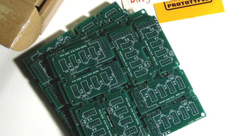
Anyone who’s made a PCB has encountered the conundrum of having to pay for space that you don’t use… for instance, designing a round PCB and seeing the corners go to waste. The solution? Smaller boards added to the blank spots.
One logical stumbling block might be that you simply don’t have a small PCB design ready to go. Latvian hacker [Arsenijs] created a resource of small PCBs that can be dropped into those blank spots, as well as a tutorial on how to combine the gerbers into a single panel.
 Great minds think alike, and this guide is following hot on the heels of [Brian Benchoff’s] article on panelization. They’re both a great read. It’s interesting to think that not long ago we would see multiple guides on home etching boards and now we’ve climbed the production ladder to guides that help better utilize PCB fab houses. Neat!
This project seems a logical spinoff of [Arsenijs]’s ZeroPhone Pi smartphone project, a finalist for the 2017 Hackaday Prize that makes a low-cost phone using a stack of PCBs. One imagines that while prototyping the phone [Arsenijs] ended up with a lot of wasted space! Fill that up with smaller designs like breakouts, or decorative items like a hackerspace business card. If you’re looking for small PCBs you can find a few in the files area of the project on Hackaday.io. Otherwise, you can share yours and [Arsenijs] will add them.


Utilising that extra space is great but all the Fab houses I have come across charge per design. So if you wanted to use up that extra corner with a useful brrskout especially something held in there with tabs and break-offs they slug you again or curate an extra fee. I would like to know some Fab houses that don’t do this, at least that would help negotiate costs down.
Some charge extra, but not all. If you price your boards on http://PCBShopper.com, you can tell it how many designs are on your PCB and it will factor that in when telling you how much each manufacturer charges. (This is assuming designs not separated by a v-groove or routing).
Disclosure: I run PCBShopper.
That site’s worth a bookmark, good work.
Could you please add aluminium PCBs to PCBShopper ? Thanks
Thanks for the link Bob I’ll certainly check that out next time. In general I try to foster a relationship with a board house, it is especially useful when trying to het through the purchasing hoops of our organisation as well as being able to push through rush jobs etc.
With services like seeed’s fusionpcb and gold Phoenix I have tried to to do can connected gerbers in the past, even running common ground and vcc traces before being rejected as multiple designs or charged an extra fee. Maybe I was just unlucky or really obvious
You can use tab (mouse-bite) routing as depicted with DirtyPCBs 2 layer boards (I don’t think you can with the 4 layer ones), no extra cost last time I looked. Stijn’s panelizer (see Brian’s article) was made specifically with DirtyPCBs in mind as I recall.
I don’t know if any of the other cheap fabs support this for free/cheap though, maybe Bob could ask fabs to submit that information and add to PCBShopper since it’s quite useful.
I can confirm that Dirty PCB charges per area, not per design. This did cost only their regular price:
https://hackaday.io/project/21097/gallery#ebe0e0a27a7fa6a90d94d901387c2428
It looks like Seeed (Fusion) will also do tab (mouse-bite) for free if there is only one design per pcb (multiple copies) and the total pcb (panel) size ordered is greater than 7x7cm, they will also do v-score apparently. But note that if there is more than one design on the pcb, then they charge (considerably) more. Google for: seeed pcb panelization rules
Yeah, by my math they charge as much as if you submitted 2 designs.
I have never had problems putting multiple designs with small tabs and no mouse bites using a few board houses.
But, in all cases the PCBs were also connected together with wires over the tab. I once made a design that required a small front panel and designed it so it can be tested together while the boards were attached.
My company gets all their prototype PCBs from Sunstone circuits. They charge by rectangular board area so you’re still paying for the gaps between PCBs.
I’m not thrilled with them lately, though. They wanted to charge an extra $200 for solder mask and my boss agreed to go without it. Sunstone still included the silkscreen for free, and I wasn’t notified at the time of the order so when the PCBs arrived I was shocked to see silscreen right there on the tin-plated ground fill. On a dense PCB for 805 SMT and 128-pin QFP packages, it wasn’t fun hand-soldering those.
Why not use somewhere like Elecrow or check on PCB shopper?
Well, they can’t exactly charge extra if they don’t know it is two designs… Put it as one set of gerbers with one board outline, and there shouldn’t be a problem. You’ll have to cut them apart yourself, but that’s OK.
They have human beings who look at the Gerbers and see whether there’s any interconnects between the circuits. It’s not foolproof, but it’s their judgement call.
Some (e.g. PCBFabExpress, who I will not use again for various reasons) will go so far as to have humans check for stuff like duplicate reference designators. And yeah, they have discretion in deciding whether that repetitive looking circuit on your Gerber is one 8-channel filter or 8 one-channel filters, and stick out their hand for extra fees accordingly. In my experience, for a board house that does this, the odds of them stopping your job to bicker about whether your board has multiple designs or not correlates very well with how much of a rush is on your order (each time they contact you with a question about your order resets the turn-time clock).
we charge by the panel. we dont care how many designs you have.as long as they are on 1 gerber we dont want to merge them ourselves
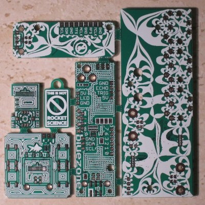
Try the GerberTools from ThisIsNotRocketScience, specifically made to panelize a set of gerber files:
https://github.com/ThisIsNotRocketScience/GerberTools