The ambitious etchr – the PCB Printer is just a concept at the moment, but it’s not often we see someone trying to tackle desktop PCB production in a new way. Creator [Jonathan Beri] is keenly aware that when it comes to creating electronics, the bottleneck for most workflows is the PCB itself. Services like OSH Park make professionally fabricated PCBs accessible at a low cost, but part of the bargain is that turnaround times are often measured in weeks.
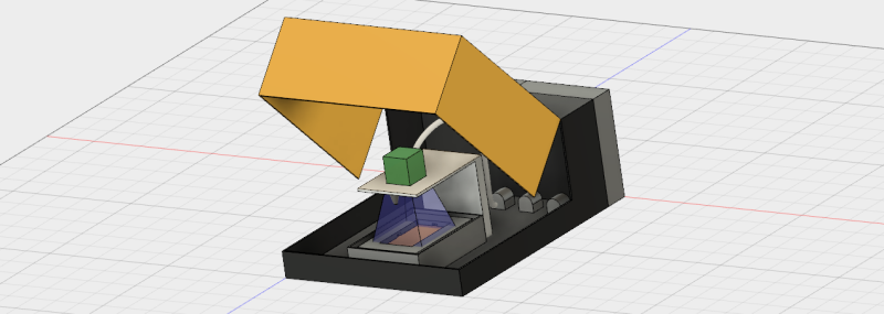
[Jonathan]’s concept for etchr is a small system that automates not only etching a copper-clad board with all the attendant flooding and draining of chemicals, but applying a solder mask and silkscreen layer labeling as well. The only thing left to do would be to drill any required holes.
The idea behind etchr is to first take a copper-clad board with photoresistive film or spray applied to it, and fix it into a frame. A UV projector takes care of putting the traces pattern onto the board (and also handles a UV-curable solder mask in a later step) and the deep frame doubles as a receptacle for any chemical treatments such as the etching and cleaning. It’s an ambitious project, but the processes behind each step are well-understood and bringing them all together in a single machine is an intriguing approach.
Desktop production of PCBs can be done in a few ways, including etching via the toner transfer method (whose results our own Elliot Williams clearly explained how to take from good to great). An alternative is to mill the PCBs out directly, a job a tool like the Othermill is designed specifically to do. It’s interesting to see an approach that includes applying a solder mask.


“S.T.E.A.M.” seriously?
Just thing of all the pretty pictures you could put on PCBs! Obviously art should be included here. ;P
Well, it’s not called board “artwork” for nothing, is it?
1++
My popcorn is stale.
What do you think about the prize entry?
Let’s discuss any flaws and suggest potential improvements to the design.
if we are going to add ‘art’, why not also history, geography, sociology, etc., and we can just call it ‘stuff’
I prefer ‘Science, Mathematics, Understanding and Technology’
Probably because of some steam punk enthusiasts. :-)
“S.T.E.A.M.” seriously?
Yup, “S.T.E.A.M.” makes me Boiling Mad! Take out the “A” and I’m all-in for the concept. But my opinion risks retribution by the “A” Fascists.
acheiving the goal would be great, but i can’t see how it can be done. As for “…Automated application of chemicals so you never have to touch them…” I can’t see this working unless you have closed cartridges, which will make it much more complicated than just having a tray full of chemicals.
I would be happy for a well made, non-sloppy, and somewhat portable or packable into reasonably portable unit ez-bake PCB kitchen set even if I had to move the boards to the next process when an alarm sounded.
From my experience with PCB milling machines, anything that still requires you to do the drilling and plating of through holes and vias yourself is not going to be worth the effort.
I love the idea of desktop PCB creation, and I hate that my first reaction when I saw this was to criticize it for what it doesn’t do, but them’s the breaks. This machine – if it works – could be used for simple single-sided boards, but anything more complicated would still need to be sent out somewhere.
This exactly. Not being able to drill and plate vias is pointless.
I can do single sided PCB protos on a breadboard. No practical high speed design will be possible in one layer.
Exactly. Cool idea, and I hate to be an arm-chair quarterback, but it misses the mark because it doesn’t produce plated vias. It’s “yet another way to make single-layer hole-free PCBs” — add it to the list of sharpie/etch, toner transfer/etch, mill with CNC machine, laser-cutter/etch, 3D print/etch, conductive-ink-print, etc.
Until someone much smarter than me comes up with a good way to do normal-sized plated vias without a complicated plating line, I’m not biting. My university’s maker space bought a $35,000 PCB milling machine, and it sits there, collecting dust. Why? For the price of lunch, I can have boards shipped from OSHPark in 4 days. That’s tough to beat, especially considering that I’ll be ordering a BOM and a laser-cut stainless steel anyway. And if I need something quickly, it’s probably for a commercial client, who has no problem paying Advanced or Sierra or whoever to overnight me something.
Then again, there’s a whole other class of people who are legitimately amused by running CNC milling machines to make PCBs from scratch — but I think that’s a phase most people grow out of. At some point, you want to focus on the creativity / problem-solving (electronics *design*) and not tedious, manual labor (electronics *manufacturing*).
There’s a whole other class of people who don’t live 4 days away from ultra-cheap services like those from OSHPark and Shenzhen.
But then they probably couldn’t afford a set up like this in place of the actual fabrication… They would still have to order parts etc as well, as someone pointed out. I’m nowhere near OSHPark or Shenzhen, but can wait a little bit and I’d have to make a heck of a lot of PCBs to offset the cost of an all in one system, and still produce a technically far inferior product. Still have to order consumables and dispose of toxic waste (both very expensive at small scale), and you have much higher wastage.
kdev has it – patterning and etching is the easy bit (although even registering top/bottom copper can be a bit of a pain), drilling is hard work (I did 500 holes with a press a couple of times, which was tedious to say the least, and highly error prone), and then no plated through holes, no copper plating or solder mask (can be a real killer for fine pitch work), no solder mask, no milling etc etc. Yep, unfortunately this doesn’t work out. Fair play as a project, but don’t expect to sell it to anyone.
That does not follow AT ALL. OSH Park clearly states a time-to-ship of up to 12 calendar days for their baseline service plus up to three weeks of shipping time after that for international orders. By that time I probably forgot what that PCB is supposed to be doing in the first place and cobbled something together dead bug style or on proto-board ages ago. Chinese fabs have similar wait times. Also, both these might involve a trip to the customs office. On the other hand, I can order almost any component I need from a major supplier that arrives to my door in 2-3 days tops no fuss, and my 3020 desktop mill can churn out simple PCBs within minutes of me designing them, drilling and outline milling included. Yes, plated vias are best avoided if possible as they need manual “plumbing” and finish is obviously not the same, but in terms of convenience it doesn’t even begin to compare.
@Max, if you’re international, you should find a more local supplier. There’s several European board houses that get stuff done inexpensively (<$60). Where are you based? Either way, if you're paying international shipping from OSHPark, might as well tick the "super swift service" box, pay a couple extra bucks, and have your boards shipped in 4 days. I used to do all my quick prototypes from Advanced Circuits with a student discount, and slower/cheaper stuff from China, but OSHPark has gotten so good the last year or two, I've switched over to them when possible. I just ordered boards on Monday, and they'll arrive in my mailbox Saturday morning. $40 for 6 boards, including shipping. I'm glad I clicked the right shipping option from DigiKey, otherwise I'd be waiting on parts!
Look up LPKF ProConduct. I mean, it doesn’t look as nice and shiny as plated though holes, but it works just fine.
@Marian, how messy/time-consuming is the process? I feel like I’ve looked at it before, and it seems super tedious and manual. I think a regular plating line (with a palladium catalyst, followed by copper electroplating) is probably “easier” — even though it’s more expensive and sort of time-consuming to set up. I think a lot of engineers like me would gladly spend an afternoon and a few hundred bucks setting up something that would allow us to dip a board in a few baths and walk away.
jaydcarlson says: “For the price of lunch, I can have boards shipped from OSHPark in 4 days …… $40 for 6 boards,”
You pay $40 for lunch!?
Not a new idea, but I never seen anyone that done it. Suppose this will stay in the concept phase…
I can’t say I’ve made hundreds of PCBs, but I didn’t think it was that hard using the usual methods. I’ve used the pre-clad boards and UV boxes, no problem, I’ve used the spray-on resists, which are less convenient but okay. Didn’t do very well with the toner-transfer method but I’ve had some good results with those special blue sheets that you use with a printer and laminator (probably my favorite method). The actual etching process always seemed fairly straightforward. Haven’t tried using a CNC machine but from what I see out there it looks like people also get very good results that way with machines costing less than a couple of hundred bucks.
just an idea to reduce the number of chemicals to 1 for the copper layer (no solder mask or silkscreen):
assume laser cutter (or perhaps stencil plotter/cutter)
assume traces occur in limited amount of orientations: perhaps only 2 (manhattan, vertical and horizontal), perhaps 4 (also diagonal directions)
for each orientation cut a (flexible?) sheet of plastic or perhaps vinyl or sticker with only cuts in one orientation:
manhattan case: 2 stencils, one only horizontal slits, other only vertical slits.
also diagonals case: 4 stencils in total, the 2 above and the 2 with diagonal cuts.
since each stencil only contains cuts in only one direction, the whole stencil remains a connected object, and no accidental hole containing part of the intended artwork could be cut out (!): if all the cuts were on the same stencil then part of the artwork could fall out in the general case
there is no UV curing or development in my proposed process:
in turn apply (adhesion? framing? pressure?) each mask to the copperclad, dunk it in coppersulphate solution, and attach a positive voltage to the copperclad, and a negative voltage to a seperate piece of copper in the same bath, the current will faradayically transport copper from the exposed (through slits) copperclad to the target copper electrode.
open problems: exact application method, alignment of mask to copperclad (2/4 masks)
in theory there is no consumable chemical so it could be used indefinitely, but in practice the coppersulphate solution will over time become contaminated with impurities in copper or dirt or dust in the air.
perhaps even 3d print the 2 or 4 stencils, such that it is solid and can be easily pressed against the copperclad. If 3d printed, also print features to attach the 3d printed stencil to the frame system (or its springs).
plastic stencils could possibly be reusable for multiple PCBs, but say stickers would have to be recut for each instance of the same PCB
The great weakness of DIY PCBs is the gnarly chemicals to etch them.
But there is no good replacement for the DIYer, and any etched board beats the pants off of perf and a mess of jumper wires.
Gotta dead-bug everything.
No. The chemicals to etch are no problem at all. Some muriatic acid and some hydrogen peroxide. In fact this substances are produced inside your own body (in low concentration). You get them in pool supply stores, etc.
The great weakness of DIY PCB is the lack of plated through holes, because of the very special chemicals you need for that.
Why don’t people just use wire?
The chemical process is the easy part. It’s drilling that is annoying and time consuming. If a solution does not handle the drilling, then it is a non-starter for me.
you mean drilling for through hole parts? or drilling for vias? I will assume drilling for vias.
perhaps instead of drilling holes, design it such that the circuit can reside on multiple rectangular (doublesided?) boards which are stacked in 2 or so layers vertically but with multiple boards side by side resting on the same board.
This way a PCB Shear would suffice. (think design for manufacturing, but just PCB shears instead of drilling holes)
I have no problem doing toner transfer and etching, it’s the hole drilling part that I despise.
I use an old ShapeOko CNC dremel to drill all of my holes as the first step, and then use the hole pattern to align the artwork on the top and bottom layers. That being said, it is the lack of plated through holes that is the real problem because it makes each via gigantic and the CAD program assumes plated through holes, so the whole thing is error prone. I rarely make my own boards anymore; I just buy them an work on something else while I wait.
so we need a home brew via rivet placement and press machine. Obviously can do drilling before hand.
Making rivets “fall” so they fit through the board, 1st time every time, would be a challenge.
Or fit rivets by hand and CNC press them? Shaking the board post pressing may dislodge loose ones tho.
Would make an interesting team project.
I made some tests before with a UV projector and got nice results.
http://hackaday.com/2016/01/07/make-pcbs-with-dlp-omg/
Anyone ever tried plasma thermal spraying the copper onto a board?
Not sure where one would obtain a high quality uv projector but it could be interesting
For me if I need a pcb right now for testing or just a simple bodge, mod or adapter board I’m willing to take the time and effort to toner transfer my own boards using some pcb tricks to easily surface mount threw hole parts and avoid drilling all together
I’m also not very worried about silk or mask
Still could be a useful tool
Just use (stripboard or veroboard or perfboard) or point-to-point wiring. Some articles make it sound that custom PCBs are the only option for wiring.
https://en.wikipedia.org/wiki/Stripboard
Thanks for the link. I had never heard of TriPad before
You are welcome. I use it often, so sometimes only few jumpers are needed even for fairly complex boards. If you need more than 3 holes per pad, just short 2 (or more) pads together.
The type of board I use also has power strips:
https://www.digikey.com/product-detail/en/vector-electronics/8023/V2040-ND/1754474
There are several varieties in different sizes etc. They are probably available for less from the usual Asian suppliers.
There was a prototype of a system similar to this but on a grid pattern where by cutting apart or bridging the islands you could route paths. I think there was software that would calculate the routing and then show which to cut or bridge. Hard to explain and don’t recall all the details :-(
I like this style. Same layout as a standard plastic breadboard so is familiar and easy to go from the breadboard to a soldered board. This is an example but they come in many flavors:
https://www.digikey.com/product-detail/en/chip-quik-inc/SBB400/SBB400-ND/5978198
That looks interesting. Are the 5 holes in a column connected togother or you must do that yourself?