Printed circuit boards have never been cheaper or easier to make. We’re not that far removed from a time where, if you wanted a printed circuit board, your best and cheapest option would be to download some proprietary software from a board house, use their terrible tool, and send your board off to be manufactured. A few copies of a 5x5cm board would cost $200. Now, anyone can use free (as in beer, if not speech) software, whip up a board, and get a beautifully printed circuit board for five dollars. It has never been easier to make a printed circuit board, and with that comes a new medium of artistic expression. Now, we can make art on PCBs.
PCB as Art
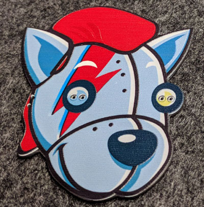
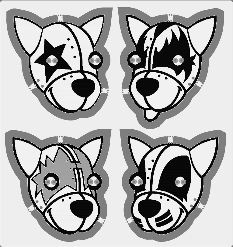
For the last year or so, Hackaday has been doing a deep-dive into the state of artistic PCBs. By far our biggest triumph is the Tindie Blinky Badge, an artistic representation of a robot dog with blinking LED eyes. [Andrew Sowa] turned some idiot into PCB coinage, and that same idiot experimented with multicolor silkscreen at last year’s DEF CON.
Others have far surpassed anything we could ever come up with ourselves; [Trammel Hudson] created an amazing blinky board using the standard OSHPark colors, and [Blake Ramsdell] is crafting full panels of PCB art. The work of Boldport and [Saar Drimer] has been featured in Marie Claire. The world of art on printed circuit boards has never been more alive, there has never been more potential, and the artistic output of the community is, simply, amazing. We are witnessing the evolution of a new artistic medium.
Printed circuit boards are a limited medium. Unless you want to shell out big bucks for more colors of silkscreen, weird colors of soldermask, or even multiple colors of soldermask, you will be limited to the standard stackup found in every board house. One color, the fiberglass substrate, will be a pale yellow. The copper layer will be silver or gold, depending on the finish. The soldermask will be green, red, yellow, blue, black, white, and of course purple if you go through OSH Park. The silkscreen will be white (or black if you go with a white soldermask). What I’m getting at is that the palette of colors available for PCB art is limited… or at least it has been.
For a few months now, Hackaday has been experimenting with a new process for adding colors to printed circuit boards. This is a manufacturing process that translates well into mass production. This is a process that could, theoretically, add dozens of colors to any small PCB. It’s just an experiment right now, but we’re happy to report some limited success. It’s now easy — and cheap — to add small amounts of color to any printed circuit board.
Defining the Problem Space
Full-color PCBs are a solved problem. A few months ago, Hackaday started talking to Makernet, a company in Shenzhen founded by [Kevin Lau]. Their raison d’commerce, apparently, is multicolor PCBs. They’ve already made full-color PCBs for Maker Faire Shenzhen, Maker Faire Xi’an, Hangzhou Mini Maker Faire, and a one-off project featuring everyone’s favorite robot dog. The process, at least on our end, for producing these multicolor PCBs was surprisingly simple: all we needed to do was send off some Gerbers and an Illustrator file; Makernet took care of everything that went into producing these multicolor PCBs.
Unfortunately, that’s all we know about how these multicolor PCBs were made. We suspect this is a UV-inkjet process, and something that could be done on a few machines we’ve specced out. If you have about $25,000 USD, you too can get the equipment to duplicate this process.
There must be a better option, and this is where we get to consider what a multicolor PCB actually means. Does the entire PCB need to be printed in full-color, or are small accents of color good enough?
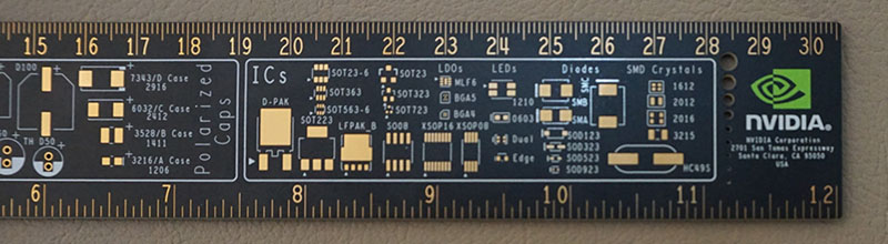
Over the last few years, companies have noticed the falling prices of PCB production and small batch electronics. PCBs are now swag for conferences and meetups. Nvidia, noticing a significant portion of their market are software engineers who have never heard of Digikey’s PCB swag, decided to design a PCB ruler. This PCB ruler measures inches and millimeters, has common footprints for IC packages, and has a few conversion tables on the back. Artistically, the most interesting part of this ruler is the lime-green Nvidia ‘eye’ logo. In contrast to every other PCB ruler out there, the Nvidia logo is resplendent, a shining example of what PCB art can do.
We don’t need full-color, full-panel PCBs for successful PCB art. The Nvidia PCB ruler proves that. The problem we’re trying to solve, then, is small, spot colors applied to a PCB. The printing area can be small; small blinky badges usually aren’t larger than 50mm square, anyway. One or two colors should be sufficient. This should be a manufacturing process, and hopefully, a process that anyone can contract out to a shop with the right equipment. There is such a manufacturing process that is perfect for multi-color PCBs. It’s called pad printing, and odds are you’re surrounded by a dozen objects with pad printing on them right now.
An Introduction To Pad Printing
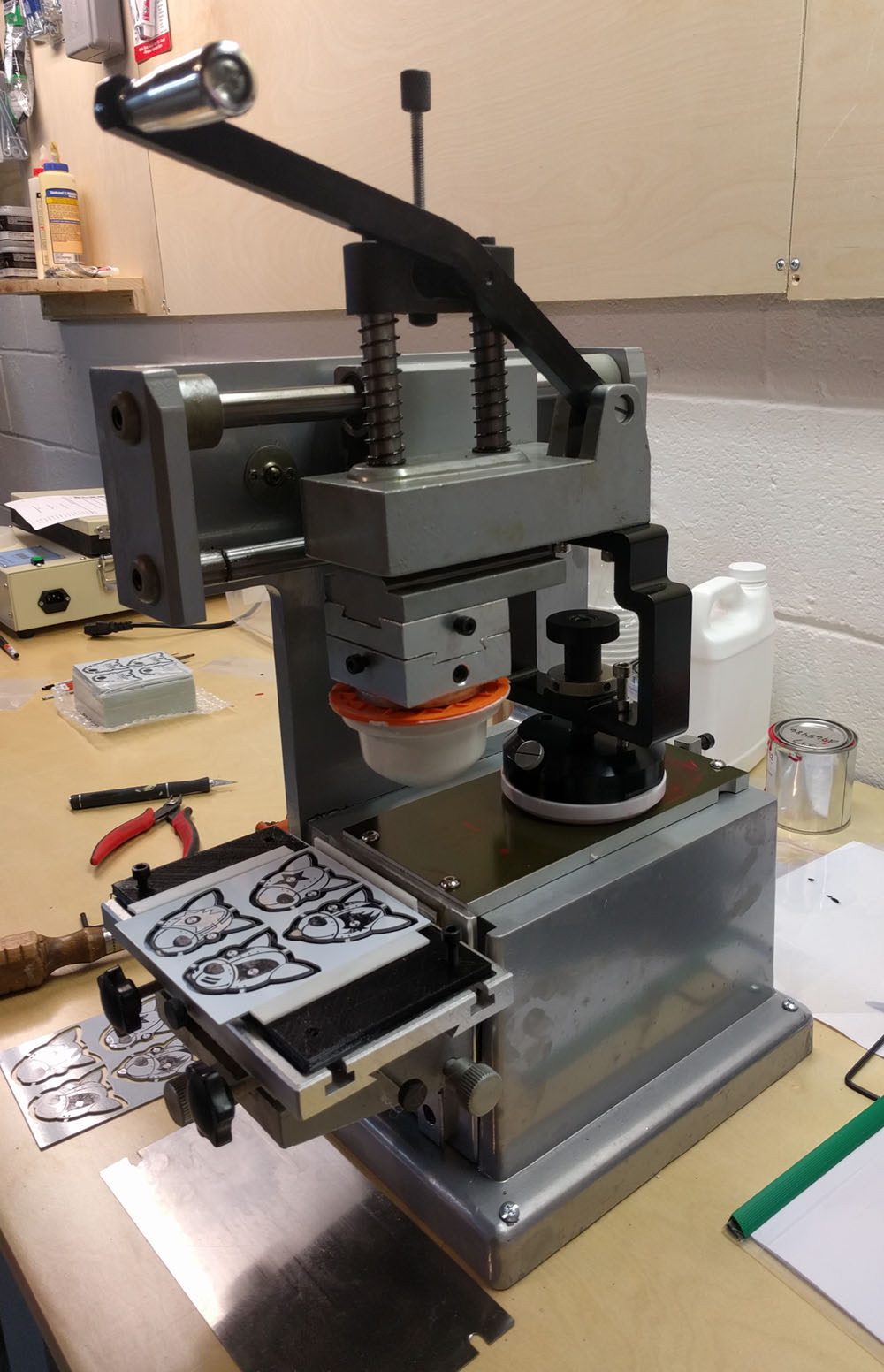
So, what is pad printing? It’s the process of using a silicone pad to pick up a very carefully shaped area of ink and apply it to an item during the manufacturing process.
It works by first making a printing plate. This is, in pad printing lingo, called a ‘cliche’. They are usually made with a photolithographic process, although you can get laser-etched plates. That printing plate then has ink wiped across it, filling the cliche with ink in exactly the design you want. A silicone rubber pad is then pressed into the cliche, picking up the ink and then transferring it to the object. You now have a pen, mug, or PCB with your logo on it. It’s that simple.
You may not realize this, but you’re probably touching something with pad printing right now. Pad printing excels at printing on curved surfaces, so if your computer mouse has some printing on it, odds are it is pad printed. Pad printing is seen on nearly every consumer electronics device, and if you’ve ever picked up a branded pen or mug from a swag table at a conference, it has certainly been pad printed. This is the process that puts flames on Hot Wheels cars, the red stripes on bowling pins, and a million other consumer products.
The ink used for pad printing isn’t terribly different from the ink used in silk screening. It’s very resilient, and it comes in a rainbow of colors. If you need a printing process that scales to manufacturing and is able to apply small areas of color to anything, pad printing is the way to go. It is, in some ways, superior to silkscreening; the cliches can be made with a laser cutter instead of the photo process of traditional silkscreen equipment.
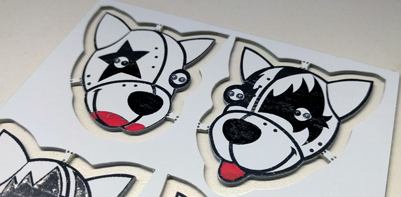
The Tindie Badge Homage to KISS
In the interests of pushing the boundaries of artistic PCBs, Hackaday has decided to experiment with the application of pad printing to PCBs. It’s not much, and the first experiment is only another Tindie Blinky Badge, but it does serve as a good example of what can be done with pad printing and PCBs. Specifically, this is a panel of Tindie badges featuring the members of the band KISS. White, black, and silver (for Ace’s face paint) are easy, but it’s really not KISS unless we can give Paul red lipstick and Gene a red tongue.

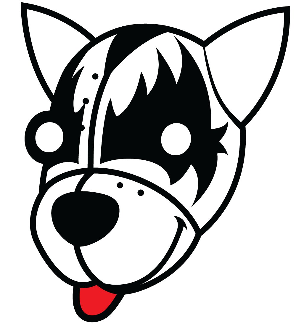
The process of creating this panel of Tindie PCBs was exactly as you would expect. Like other Tindie blinky badges, this was designed first in Illustrator by Hackaday’s resident artist [Joe Kim]. It was then imported into Eagle. Here’s our walkthrough on how this art was translated into fiberglass, copper, soldermask and silkscreen. The only significant difference between these KISS Tindies and our earlier badges is another layer of Gerbers. This layer is only where the red should be applied by a pad printing process.
After receiving the manufactured KISS Tindie panels from DirtyPCBs, we only had to take the ‘red’ layer of Gerbers, print them out on a transparency, create the pad printing cliche, and lay some ink on the PCBs.


A Successful Experiment
The experiment was successful, albeit with a few problems. It took some effort to figure out the correct temperature for the ink, how much thinner to use, and a how to deal with a slightly dirty silicone pad. But with that sorted, we can apply spot color to a stack of PCBs, vastly increasing the palette for PCB art.
The total cost for this experiment was about $1500 for all the equipment including a UV plate exposer, consumables, and the pad printer itself. This is a very cheap pad printing setup — the simplest automatic pad printing machines start at around $4000, with machines able to print larger areas and multiple colors going up to $20,000. Of course, pad printers are ubiquitous in manufacturing environments, and used equipment is always an option.
Additionally, because pad printing is a common manufacturing process, this is something that could be contracted out. Think of all those branded pens you pick up at conferences. They all came out of pad printers, and there is most likely a shop with a pad printer near you looking for business.
Is this the solution for multi-color PCBs? Well, it’s a solution. There is no silver bullet for the problem of creating artistic PCBs. If, however, you only need a few bits of color on your PCBs, pad printing is an effective and cheap method of extending the possibilities in the world of PCB art.


but i’m looking to do some foil embossing, holographic patterns, halftone op art, and lenticular prints on boards!
This sounds very similar to fingernail stamps. A metal plate with a design etched gets some polish dripped on it to fill the design and then a silicone “stamper” is pressed on to the plate to pick up a bit of the polish and finally press it on to the fingernail.
A quick Google search shows that an UV printer like the UJF-7151plus costs $13k ( http://bestprinterasia.com/index.php?route=product/product&product_id=297 ). There might be an opportunity to provide a color print service for PCBs.
But of course, there are already services which print anything with such an UV printer. E.g. one costs $50 for a 6.5″ x 20″ area, plus a setup fee of $30 and minimum order of $150 ( http://www.factoryenova.com/sp/pages.php?pID=70&CDpath=21 ). So for a 5cm x 5cm conference badge, you can fit 30 badges on one half bed size for $50. The setup fee doesn’t matter if you need e.g. 300 badges. Then it would be only $1.80 additional cost per badge. Anyone who wants to try it?
You can do the calculation yourself how many PCB with prints you need to sell, if you want to buy your own printer. But the ink costs a bit as well, like $200 per 1 liter bottle.
Is there a reason you tried this over UV silk screening?
I’m not going to say that UV silk is harder. They’re probably the same amount of effort. But pad printing has a few things going for it.
You can mix colors, which means you have an infinite variety of colors. I don’t know how that works with UV silk screening. The startup costs are smaller for pad printing (~$1500 for the first plate, and about $5 per plate afterwards (or color in one design)). Given that pad printing is errywhere, this is something that can be contracted out easily. That’s probably not true with UV silk. You’re beholden to your board house at that point.
It’s a solution. I’m not saying it’s the best, but it’s cheap, easy, and you can screw around with it. The ultimate goal of these pad printing experiments is the cover of Mellon Collie and the Infinite Sadness. Let me get to that point and I’ll tell you how easy and effective this actually is. Of course, I still think a UV printer is still the best way to go here.
Nice work Brian! Thinking back on the UV theme, could (thinned?) UV cured nail polish provide a source of full-pallette colour? Perhaps printed or stencilled over white silkscreen backdrops?
Sending the boards to a contract silk-screen printer might be another option. Since you’re printing on a flat surface, the pad printing may be overkill.
For home stuff, one could cover the whole board with UV soldermask paint, selectively expose areas using whatever method you prefer (transparency film + UV lamp, laser diode on 3D printer, projector, etc.). Then just repeat with next color.
Or, you could roll your own and get the product you want instead of the limited products of the “board houses”…
Another easy way would be a sticker, with laser cut holes when needed for parts.
That’s really cool, I hadn’t known about Pad Printing. I have been increasingly interested in UV printing over the past couple years or so, myself. One frustrating thing I learned much slower and later than I should have is that when talking to industry people they’ll often tell you such-and-such can’t be done, but what they MEAN is that their machine or shop doesn’t do it, not that it cannot be done. Sooner or later if you want to fiddling with a thing, you reach the point where you just have to buy the equipment. At times like that a $500 investment for a basic, manual machine is much more accessible than say 15,000!
yeah, I can do full CMYKW on pcb with UV inkjet BUT there is nobody to sell me proper CMYKW inks for soldermask with chemical and mechanical resistance (and proper adhesion). There is only green agfa (..soon) and ultraglossy black from tayio. No other options.
Black+white inks are only for labels. Magenta ink from agfa is “printable solder resist” easly dissolved by NaOh.
Another problem, not single PCB software support real-rgb colors in layers.
My color tests:
http://plosnaky.cz/img/sample/colors2.jpg
http://plosnaky.cz/img/sample/colors3.jpg
The ads say UV printer ink sticks to anything like plastic, metal, glass, fabric etc. Maybe try without solder mask, if possible (like no fine pitch ICs)? Then it would be only plastic for the board and the copper for the traces.
“ads say” – they peeling off, maybe bad ink company. Printing on metal is difficult, surface needs to be chemically prepared. Those uv inks are unable survive aceton or NaOh or CuCl2 or high heat (like reflow) – every color is different. Another story is, that commercial piezo head are heated with circulating ink. For example agfa dipamat ink has too low viscosity (too much sticky) and my printer head can’t handle it.
That info really highlights how as usual, things can look simple from the outside but always the devil is in the details.
What would be your preferred export format from layout software that supported RGB attributes in layers? Gerber, postscript, PNG, pdf, etc… ?
Just curious.
I’m using cmyk postcript.
Gerber has origin and exported image for printer should respect same origin and somewhere should be information how far is image from it.
top mask file: top.png
top mask x offset: 13.500
top mas y offset: -60.800
Man, I want that nVidia ruler. Shame they’re all about £100 on ebay :(
mimimimimimimi. No word about my multicolor spacehuhn badge, I’ve handpainted them with some Edding pens.