
We were musing upon the relative paucity of education with respect to the fundamentals of electronic circuitry with discrete semiconductors, so we thought we’d do something about it. So far we’ve taken a look at the basics of transistor biasing through the common emitter amplifier, then introduced a less common configuration, the common base amplifier. There is a third transistor amplifier configuration, as you might expect for a device that has three terminals: the so-called Common Collector amplifier. You might also know this configuration as the Emitter Follower. It’s called a “follower” because it tracks the input voltage, offering increased current capability and significantly lower output impedance.
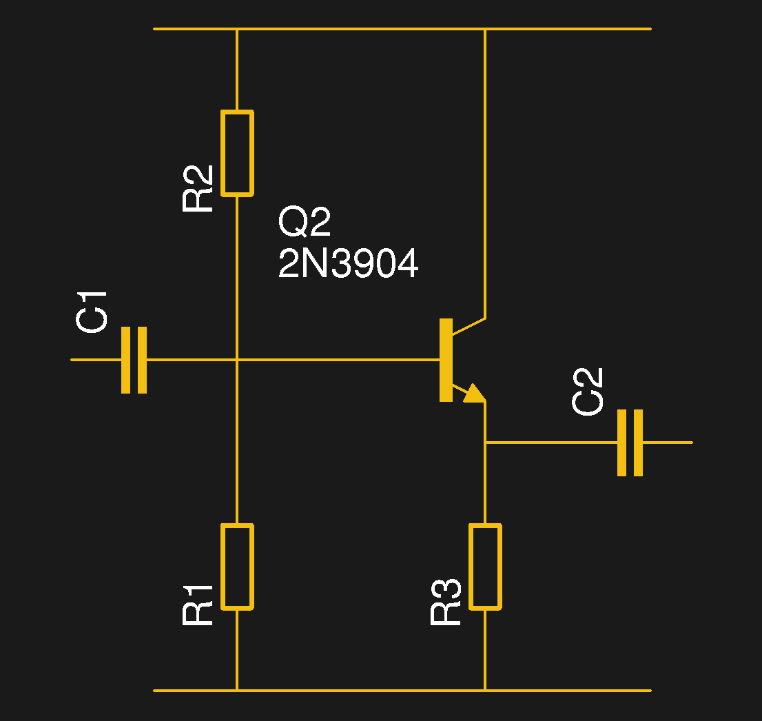
Just as the common emitter amplifier and common base amplifier each tied those respective transistor terminals to a fixed potential and used the other two terminals as amplifier input and output, so does the common collector circuit. The base forms the input and its bias circuit is identical to that of the common emitter amplifier, but the rest of the circuit differs in that the collector is tied to the positive rail, the emitter forms the output, and there is a load resistor to ground in the emitter circuit.
As with both of the other configurations, the bias is set such that the transistor is turned on and passing a constant current that keeps it in its region of an almost linear relationship between small base current changes and larger collector current changes. With variation of the incoming signal and thus the base current there is a corresponding change in the collector current dictated by the transistor’s gain, and thus an output voltage is generated across the emitter resistor. Unlike the common emitter amplifier this voltage increases or decreases in step with the input voltage, so the emitter follower is not an inverting amplifier.
The keen-eyed reader will have noticed at this point that since the base-emitter junction of a transistor is also a diode, it will always maintain approximately the same voltage across itself regardless of the current flowing within it. For a silicon transistor, this is around 0.6 V so the output voltage on the emitter will always be 0.6 V lower than the input voltage on the base. Thus the voltage gain of an emitter follower will always be just a tad less than 1, and you might thus expect that it would therefore be of little use as an amplifier if you neglected that it has significant current gain. The output impedance of an emitter follower is significantly lower than that of a common emitter amplifier, allowing it to drive much more demanding loads. You will often find it used as a buffer stage for this reason, and a handy example can be found on the output of an early op-amp we took a look at earlier in the year.
We’ve now taken a look at the three basic configurations of a transistor amplifier, as well as the fundamentals of biasing a bipolar transistor. It might seem odd to cover this topic on Hackaday when it’s certain that many of you are already familiar with it, but sometimes it’s worth remembering that not everybody is fortunate enough to he well-versed in these fundamentals. The impetus for this series came from a friend lamenting that while his pupils had advanced knowledge of microcontrollers that his generation hadn’t acquired as their age, they had not been given the opportunity to learn these fundamentals.
There is one final piece to come on this topic, these same principles apply to the other three-terminal active components, so we’ll have a quick look at FETs and tubes.


Pacman was here and ate all the dots.
Right. And I always felt that Pacman should be kept away from beginners diagrams….. or any, for that matter
or else Pacman may get zapped …
I love how everyone is complaining about the dots, but nobody offers to correct it.
While I liked the minimalism, you need to be more detailed when handing a circuit diagram over, and the assumptions you make.
Feel free to use this, 5 minute mspaint edit.
https://i.imgur.com/p7iMYPS.png
Jenny, these articles are great! I took the opportunity to glance through them again, and noticed that there’s still a correction that hasn’t been made in the first article on the common-emitter amplifier: in the 4th paragraph of that article, it should be discussing the base-emitter junction, not the base-collector junction. These articles are a great resource to pass to someone just learning about transistor amplifiers, and since not everyone takes the time to read the comments, it’d be great if we could make that correction!
Again, love this work. Nicely done.
Honestly I think the ones with spice are better. Don’t know why these are different.
I addressed this point in the comments, I think it’s a matter of language. Please take a look.
And thanks.
Jenny, I love this series, but paragraph 4 of the common emitter biasing discussion should say, “In an NPN transistor, the connection between base and emitter is a PN junction, so as you might expect it shares its properties with the PN junction in a diode. A silicon diode starts to conduct when the voltage across it reaches about 0.6 V, and when the voltage from our potentiometer across our base-emitter junction reaches 0.6 V, it also starts to conduct.
You may not be looking at the paragraph we’re all trying to get corrected. Your comment adressed paragraph 2, but the problem is in paragraph 4.
this seems to be turning into a running gag…
Very distracting without the dots…
Very distracting indeed. Add some dots!
“We were musing upon the relative paucity of education with respect to the fundamentals of electronic circuitry with discrete semiconductors, so we thought we’d do something about it.”
Is that really because of a lack of information? Wasn’t the internet suppose to be the great equalizer when it comes to information?
People don’t know what they don’t know, so they can’t search it out without being reminded of what they don’t know.
What search string would you use to research a topic you don’t already know?
The same could be said for these articles. What search string would people use to find these articles and how would it be different from those used to find it elsewhere?
but you dont need to search to find these articles, if you have an interest in electronics , read this blog, and these articles fill a hole in your knowlege, then thats the difference.. its liek watching some old timer mechanic on youtube, he shows you a trick to remove a stuck bearing thats “common knowlege” amongst the old guard but a new person finding their feet will not know to search for it, as they dont know its a thing.
What’s missing is an article on push-pull stages, and then it’s possible to do the hello world of analog electronics: an audio power amplifier. For new people to get interested you need to give them a reason to get building the circuits.
I’d suggest the series complete covering the basic Class A amp, in FETs and valves.
After that, cover push-pull as the subject moves through Class AB, B, C, and eventually Class D.
The series isn’t yet over. :)
I would add one more thing to that: it is possible to connect output of common emitter stage directly to common collector stage without biasing resistors – bias is adjusted at common emitter stage in such a way that at the output of emitter follower DC voltage is at half of supply voltage, and current flowing trough the first transistor is at least ten times higher than minimum base current of the second transistor (≈ Ie * βmin)…
There’s a handy trick for reducing the voltage offset between an emitter follower’s input and output: put an NPN follower in series with a PNP follower.
Assuming the NPN is the input, its emitter will sit about 0.6V below its base. If you DC-connect that emitter to the base of a PNP, the PNP’s emitter will be about 0.6V higher. The Vbes cancel, putting the PNP’s emitter voltage near the input voltage.
The match isn’t perfect, and you need 0.6V of headroom above and below the input/output voltage for the circuit to work, but it’s handy when you don’t want to futz around with the offset.
If you take two of those, one NPN-PNP and the other PNP-NPN, you can connect the emitters of the two output transistors to make what’s called a ‘diamond buffer’.. very useful.
One correction, the voltage gain is not almost one because of the 0.6v drop, the voltage gain is exactly one, with a 0.6v offset.
Vbe will change with Ib, the higher Ib, the higher Vbe, and that’s not a linear relationship. This also introduces some distortion, and the only way to fix it is to replace the emitter resistor with current source…
A BJT’s dynamic resistance equals the thermal voltage (about 26mV) divided by the collector current. At Ic=1mA, the dynamic resistance is about 26 ohms.
The dynamic resistance shows up between the base and emitter, making a voltage divider. The emitter voltage will always by Vb*Re/(Re+Rm), where Rm is the dynamic resistance. As long as Rm is greater than zero (which it always will be) the voltage gain at the emitter will be less than 1.
I have used emitter follower design but as a very low budget (and very inefficient) volt regulator. Unregulated in to collector, resistor from collector to base, zener diode in reverse bias from base to ground, and emitter is the regulated output.
Just saying found this wasn’t actually looking. will be a handy resource.
I think it’s quite interesting to learn more about the active components of an amplifier here. Thanks.
Jenny,
I love this series of articles on the basics of transistors. It’s in the same spirit that I’ve been writing my site on valves (wtfamps.com). Hackaday covered one of my projects a year or two ago. Please feel free to cite/borrow anything you find useful on my site when you cover valves (I have a bit on FETs as well, but mostly from a valve-centric perspective).
Why not simply bias the transistor slightly above the desired output voltage to account for the .6V drop?