In a field where components and systems are often known by sterile strings of characters that manufacturers assign or by cutesy names that are clearly products of the marketing department and their focus groups, having your name attached to an innovation is rare. Rarer still is the case where the mere mention of an otherwise obscure inventor’s name brings up a complete schematic in the listener’s mind.
Given how rarely such an honor is bestowed, we’d be forgiven to think that Sidney Darlington’s only contribution to electronics is the paired transistor he invented in the 1950s that bears his name to this day. His long career yielded so much more, from network synthesis theory to rocket guidance systems that would eventually take us to the Moon. The irony is that the Darlington pair that made his name known to generations of engineers and hobbyists was almost an afterthought, developed after a weekend of tinkering.
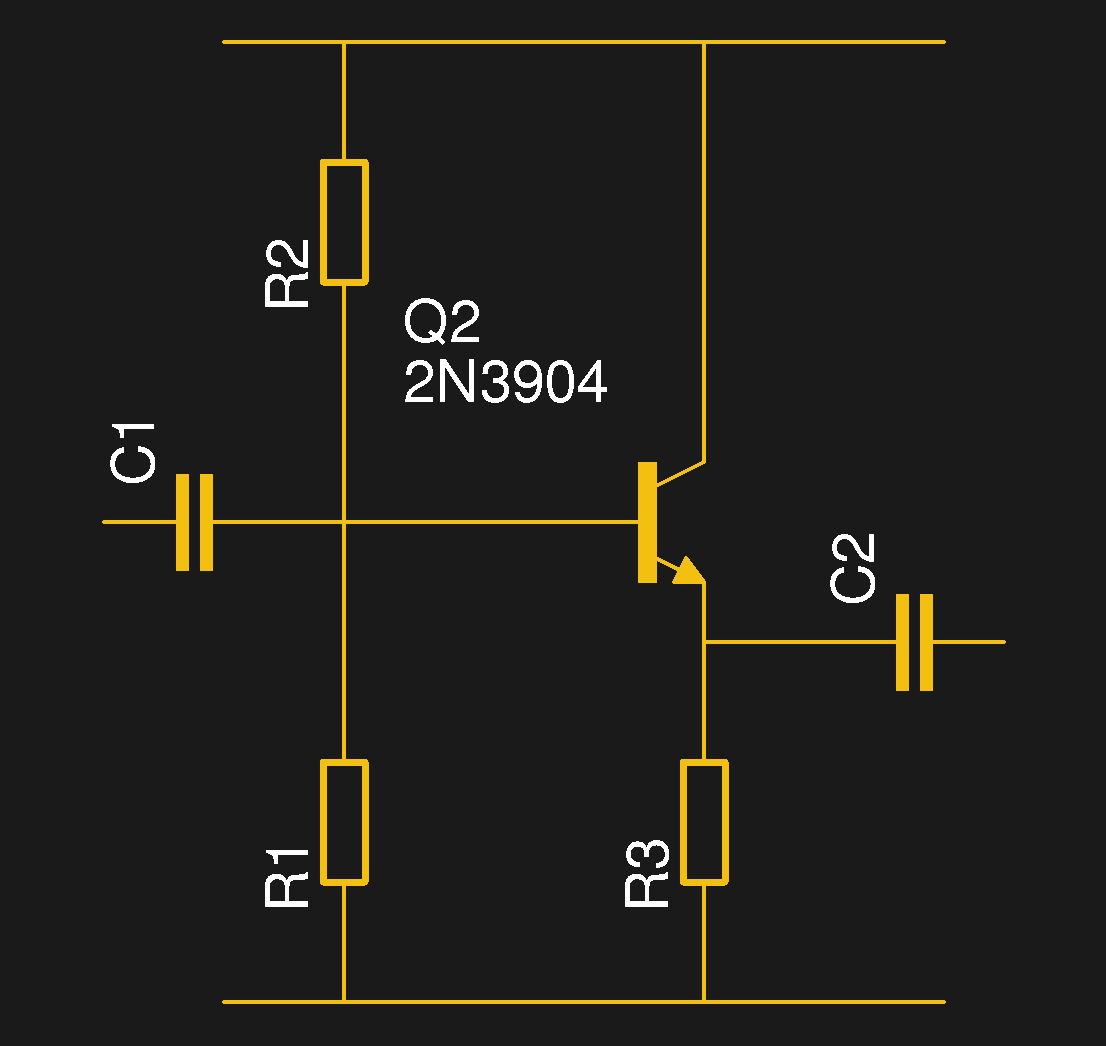
Last time on Circuit VR, we looked at creating a very simple common emitter amplifier, but we didn’t talk about how to select the capacitor values, or much about why we wanted them. We are going to look at that this time, as well as how to use a second transistor in an emitter follower (or common collector) configuration to stiffen the amplifier’s ability to drive an output load.
Several readers wrote to point out that I’d pushed the Ic value a little high for a 2N2222. As it turns out, at least one of the calculations in the comments was a bit high. However, I’ve updated the post at the end to explore what was in the comments, and talk a bit more about how you compute power dissipation with or without LTSpice. If you read that post, you might want to jump back and pick up the update. Continue reading “Circuit VR: A Tale Of Two Transistors”→
Just as the common emitter amplifier and common base amplifier each tied those respective transistor terminals to a fixed potential and used the other two terminals as amplifier input and output, so does the common collector circuit. The base forms the input and its bias circuit is identical to that of the common emitter amplifier, but the rest of the circuit differs in that the collector is tied to the positive rail, the emitter forms the output, and there is a load resistor to ground in the emitter circuit.
As with both of the other configurations, the bias is set such that the transistor is turned on and passing a constant current that keeps it in its region of an almost linear relationship between small base current changes and larger collector current changes. With variation of the incoming signal and thus the base current there is a corresponding change in the collector current dictated by the transistor’s gain, and thus an output voltage is generated across the emitter resistor. Unlike the common emitter amplifier this voltage increases or decreases in step with the input voltage, so the emitter follower is not an inverting amplifier.