It’s said that the electronic devices we use on a daily basis, particularly cell phones, could be so much smaller than they are if only the humans they’re designed for weren’t so darn big and clumsy. That’s only part of the story — battery technology has a lot to do with overall device size — but it’s true that chips can be made a whole lot smaller than they are currently, and are starting to bump into the limit of being able to handle them without mechanical assistance.
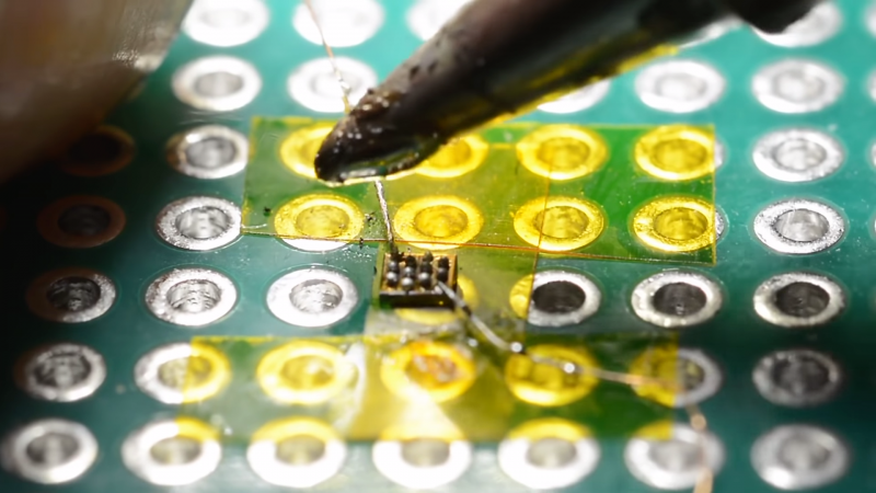
Or perhaps not, if [mitxela]’s hand-soldering of a tiny ball-grid array chip is any guide. While soldering wires directly to a chip is certainly a practical skill and an impressive one at that, this at least dips its toe into the “just showing off” category. And we heartily endorse that. The chip is an ATtiny20 in a WLCSP (wafer-level chip-scale package) that’s a mere 1.5 mm by 1.4 mm. The underside of the chip has twelve tiny solder balls in a staggered 4×6 array with 0.4 mm pitch. [mitxela] tackled the job of soldering this chip to a 2.54-mm pitch breakout board using individual strands from #30 AWG stranded wire and a regular soldering iron, with a little Kapton tape to hold the chip down. Through the microscope, the iron tip looks enormous, and while we know the drop of solder on the tip was probably minuscule we still found ourselves mentally wiping it off as he worked his way across the array. In the end, all twelve connections were brought out to the protoboard, and the chip powers up successfully.
We’re used to seeing [mitxela] work at a much larger scale, like his servo-plucked music box or a portable Jacob’s Ladder. He’s been known to get small before though, too, like with these tiny blinkenlight earrings.


I’m impressed!
Hmm, um I’ve not done chips this small though probably will sometime in next few weeks and sure it’s good practice as well as showing how tough it can be but, wouldn’t it be a fair bit quicker and perhaps a bit nicer to dab the end of the wire in some solder paste first (as well as maybe having the wire pretinned/dipped so the solder paste wets better such as if the paste a bit old) ?
I was thinking the same thing. Some solder paste, or simply some flux.
Don’t use the solder paste I recently used, it has tiny solder balls inside that get loose when heat is applied and run all over the circuit board, including wedging themselves between the leads of nearby IC’s.
Really Ren ?
And what is this mythical product you used as all good quality and perhaps common reputable ones have a specification describing very small “balls” indeed ie they tend not to ‘ball up’ – got a trade name or supplier to track this so we are enlightened by your specific experience you alert us to ?
https://www.amazon.com/Solder-Paste-Lead-Free-Temperature-ChipQuik/dp/B0195V1QEI/ref=sr_1_4?ie=UTF8&qid=1530035006&sr=8-4&keywords=Chip+Quik+solder+paste
Now, I remember, I was trying to use it to remove an IC, and it ran its little balls all over the place rendering the PCB useless!
I had a bottle of liquidy-gel stuff like that, I was trying to figure out how to filter it when I spilled the entire thing on my shirt. I had to throw it away. little lead balls and sticky brown flux make for a hard to clean stain.
me too. i am currently getting into SMD myself. bought a hot air station and tools.
tried myself on a DSBGA-25 (0.5mm pitch), failed horribly, tried again, failed again.
now i have to wait for more chips, since they come pre-balled and i cannot re-ball the others again myself.
that shit is tiny as hell…
Reballing is fairly simple. Get a reball stencil from ebay or aliexpress for it (or one that is close enough) and some solderpaste. Remove all solder from the chip, align the chip and stencil, smear solderpaste into the holes, heat with hotair until the solder is molten. Let it cool down and remove the chip from the stencil.
See here a random video doing this: https://www.youtube.com/watch?v=3bptqLxB2es
It’s impressive in a similar way to building tiny dioramas out of surface mount resistors. Impressive, but not horribly useful. CSPs with such a small number of balls don’t require super tolerances in your PCB.
His steady hand and patience is very cool. I’m thinking though, if he’s going to do this a lot, he should invest some time creating a pair of heated tweezers.
I’m replying to your comment just so people will look and say, “Hey! It’s Ren and Stumpy!”
B^)
Hey! It’s Ren and Stumpy!
Thank you [Shannon]! My life is now complete!
B^)
Shut up, you fool (slap!)
This is so painful to watch…
I don’t want to seem like I’m complaining, but how someone can do such a hard work without at least a clean tip and a liberal amount of flux is beyond me.
1+
The tip IS clean, except for the melt on it needed for heat transfer. That looks like a pretty large melt, but, again, given the magnification, it may be a lot smaller than it appears The magnification due to the microscope makes everything look horrid and out of scale. You get used to it.
I can’t speak for flux here, but I would probably go without, as well, with the wire strand tinned, then add a little if needed, most likely by heating the wire end and dipping it in paste. But that is me. I have only tried work on this scale a few times, with inconsistent success.
The excess of soldering provides a better thermal contact between the iron tip and the wire.
So, Do better! Post a video of yourself doing it and show us how it’s done!
3x3mm and 100 pads on our Nordic NRF52840
Attempted to solder it… Gave up :)
Agreed, I’ve seen those NRF52840s… they’re tiny! Something a little bigger would be nice.
SMD sub rice grain size. For a prototype batteri manager. Super glued them to a unclad board dead bug style and intended to Soldier hairthin Cooper Wire between Them! Ended as a burnt smelly 100$ mess.
The amount of soldering like this I’ve mentioned, “Pfft… this is easy, I could do smaller!!!” here on Hack A Day * ….
This’ll be the 1st time I have to admit, this looks a little too small for my skill-level.
This is some DAMN GOOD SOLDERING SKILLS!!!! (:-D)-{–{
.
.
.
*Using my old alias’ before they (and some other poor victim’s alias’s) got hijacked by some sad troll :-(
I did this for my phd prototype: 8×8 bga, pitch 0,5mm.
In my [humble,honest] opinion, THAT should have been your Ph.D.!
B^)
A lot of good points have been made, however this takes me back to a time in the 1960’s when I had to make some needed repairs using a nail in a rubber ball as a soldering iron heating it on a gas stove. The whole process was so tedious I suffered through the entire video. An answer to this is an old trick of mine to take a safety pin and cut it off at the coiled end leaving only the coil and the sharp point, then bend a 90 degree turn at the coil and literally screw it up on the soldering iron tip. Now you have a tiny soldering iron tip just the right size for the job. I invented this year’s ago to deal with first generation SMD components when they actually had legs. Laurin
P.S. I am still cringing after watching this painful process.
Hmmm, I’m wondering if/how you were able to “tin” the tip of the safety pin.
I have made some ASIIC art before (http://www.instructables.com/id/ASIIC-ART/) therefore I think soldering such sized bgas is perferctrly feasible. I would use a thinner enameled wire and less solder on the ball contacts. I would also start from the inner contacts.
https://cdn.instructables.com/F96/KSR1/H742IIY0/F96KSR1H742IIY0.LARGE.jpg
… all I see are an alive bug and a dead bug …
My 1st thought was “why not hot air gun?”. Keep solder balls melted. Touch it with wires.
Fine for the first wire, but then you start pinging wires off as you apply additional wires. I guess if you somehow have the wires want to spring into the exact right place you’d be fine, but I guess that would be true no matter which soldering technique you use.
The goal is to have it still work at the end. Heating it for that long will likely kill the chip.
Seems like that would work if you first tinned all the wires, pre-bent and taped them all in place, just touching the tops of their respective balls while having only a bit of downward pressure, and then heated them all in one go and be lucky enough that the air doesn’t displace anything.
Metal expansion probably will cause the ends to move away from the designated IC pads
Kind of reminds me of some types of surgery. Going through a waldo since even human hands move just a little.
That’s cool, but painful to watch. Like a beetle stuck on it’s back.
Maybe I am missing something here but, if the idea is to actually use the chip rather than just showing off soldering skills, wouldn’t it be easier to get a breakout board made and reflowing the chip? It is easy to design such a board and they are dirt cheap. The only downside is the time delay while they are made.
“The only downside is the time delay while they are made.”
It looks like you’ve answered your own question…
Make your own?
Reminds me of this guy, as well…
https://hackaday.com/2016/10/10/ne555s-smd-prototyping-is-a-work-of-art/
That wlcsp soldering skill level is beyond my grasp…
wow! arduous just to watch, moreso, I’m sure, in the doing, but was learning all the way through!
for the love of all that is good, please use more flux while soldering!!!! i’m literally cringing at all the poorly wetted solder right now. i routinely do this kind of dead bug chip scale work for fast prototypes and testing, and honestly half of those joints are probably going to break, fail, or aren’t actually conductive (from experience). a smaller tipped soldering iron is almost a requirement to do this correctly – as you might notice, it’s hard to get a large tip close enough to the actual pad to conduct enough heat to melt and wet the solder ball without accidentally melting the other balls. flux would have made that noticeably easier, though.
My solution was to bundle a load of enabled wire cut the ends cleanly and use them like pogo pins. Clamp the chip down on top and at least one of the wires will be in the right place for each pad. Doesn’t always work but I shake too much to contemplate doing it by hand any other way.
I wonder if a 3d printer would have the dexterity to glue copper wire in place.
Likely nowhere near the accuracy needed. Though someone is attempting a parts pick and place on the same platform. http://www.firepick.org/
Ok. I don’t need to buy an adapter board for my QSOP-8 (0.65mm pitch) chips I just got (thinking they were SOP or something). They have LEGS, should be easy!
used to do similar of it alot without scope, cause my sight degrade n eventually change lens due over myopia.. :(