Now that these DLP printers are cheaper and more widely available, we’re starting to see hackers poking around the edge of the envelope to see what else the machines are capable of. [Electronoobs] recently got his hands on a couple of these printers, and thought he would do some experiments with using them for PCB production.
 Rather than extruding molten plastic, these printers use light to cure resin layer-by-layer. In theory if the printer is good enough to cure the light-activated resin for a high resolution print, it should be able to do much the same thing with photosensitive PCBs.
Unfortunately, getting an STL out of a PCB design program takes a few intermediary steps. In the video after the break, [Electronoobs] shows his workflow that takes his design from EasyADA and turning it into a three dimensional object the DLP printer will understand. He does this with Blender and it looks pretty straightforward, but in the past we’ve seen people do similar tricks with Inkscape if that’s more your style.
Once you’ve grafted another dimension onto your PCB design, you may need to scale it to the appropriate size. [Electronoobs] notes that his STL for a 60 mm wide PCB came out of Blender as less than 2 mm wide, so you might need to break out the dreaded mathematics to find the appropriate scale value. Once the dimensions look good, you can load this file up into the printer as you would any normal print.
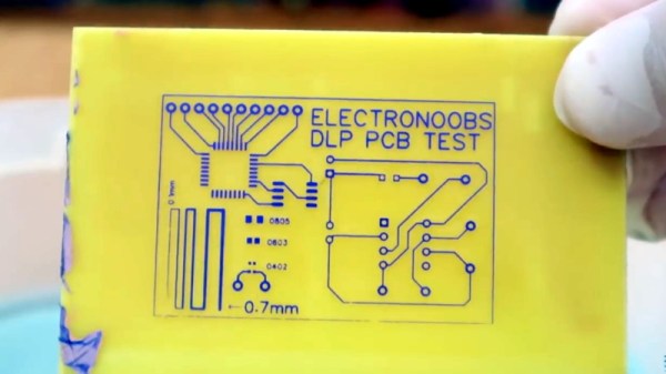
On the printer side of things, [Electronoobs] manually laminates UV photoresist film onto some copper clad boards with an iron, but you could skip this step and buy pre-sensitized boards as well. In any event, you drop the board where the UV resin normally goes, press the print button, and wait about ten minutes. That should give it enough time to expose the board, and you then proceed with the normal washing and acid bath process that hackers have been doing since time immemorial.
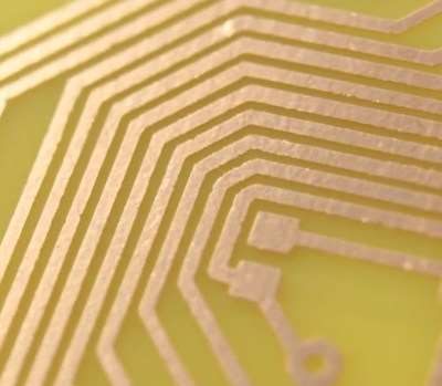
As [Electronoobs] shows, the results are quite impressive. While this still won’t make it any easier for you to do double-sided PCBs in the home lab, it looks like a very compelling method for producing even SMD boards with relative ease. This isn’t the first time somebody has tried using a DLP printer to run off some PCBs, but now that the technology has matured a bit it looks like it’s finally becoming practical.


