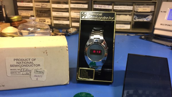
Electronics enthusiasts have the opportunity to be on the very cusp of a trend with vintage digital watches (VDW). Vintage digital watches are those watches that from the late 70’s and throughout the 80’s. They’re unlike any watch style today, and for anyone around when they made their debut these deliver a healthy dose of nostalgia.
Monetarily speaking, it is not worth the money to pay a watch maker to restore a digital watch but for those of us with basic electronics skills we can put the time and effort into making them run again and be one of the few in possession of functioning VDW. It’s a statement as well as a sign of your own aptitude.
The build relies on an astounding number of ultrasonic transducers – 72, in fact. The device operates at 40 kHz to be well above the human range of hearing. 36 each are placed in the top and bottom shells of the device’s 3D printed chassis. Through careful construction, the transducers are placed an integer multiple of half the wavelength apart. This allows the device to create a standing wave, with several low-energy nodes in which small objects can be levitated. In this case, [Julius] uses small scraps of styrofoam, but notes that water droplets can also be used if one is careful to avoid spilling any on the electronics.
The transducers are energised with a square wave generated by an Arduino Nano. This allows the possibility of the frequency and phase of the wave to be altered, which can help tune the device and allow some movement in the vertical axis. Unfortunately, movement in the other axes isn’t possible as the transducers appear to be connected in parallel. However, this could be a good upgrade in a later revision.
This project shows that a device relying on incredibly precise measurement and control can now be constructed at home with a 3D printer and some off the shelf electronics.
Right now, we’ve got artistic PCBs, we’ve got #badgelife, and we have reverse-mounted LEDs that shine through the fiberglass substrate. All of this is great for PCBs that are functional works of art. Artists, though, need to keep pushing boundaries and the next step is obviously a PCB that doesn’t look like it has any components at all. We’re not quite there yet, but [Stephan] sent in a project that’s the closest we’ve seen yet. It’s a PCB where all the components are contained within the board itself. A 2D PCB, if you will.
[Stephen]’s project is somewhat simple as far as a #badgelife project goes. It’s a Christmas ornament, powered by two coin cells, hosting an ATTiny25 and blinking two dozen LEDs via Charlieplexing. The PCB was made in KiCAD, with some help from Inkscape and Gimp. So far, so good.
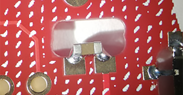
Castellated edges, containing a part
The trick is mounting all the components in this project so they don’t poke out above the surface of the board. This is done by milling a rectangular hole where every part should go and adding castellated pads to one side of the hole. The parts are then soldered in one at a time against these castellated pads, so the thickness of the completed, populated board is just the thickness of the PCB.
The parts used in this project are standard jellybean parts, but there are a few ways to improve the implementation of this project. The LEDs are standard 0805s, but side-emitting LEDs do exist. If you’d like to take this idea further, it could be possible to create a sandwich of PCBs, with the middle layer full of holes for components. These layers of PCBs can then be soldered or epoxied together to make a PCB that actually does something, but doesn’t look like it does. This technique is done in extremely high-end PCBs, but it’s expensive as all get out.
Still, this is a great example of what can be done with standard PCB processes and boards ordered from a random fab house. It also makes for a great Christmas ornament and pushes the boundaries of what can be done with PCB art.