The hackers over at Radiona.org, a Zagreb Makerspace, have been hard at work designing the ULX3S, an open-source development board for LATTICE ECP5 FPGAs. This board might help make 2019 the Year of the Hacker FPGA, whose occurrence has been predicted once again after not quite materializing in 2018. Even a quick look at the board and the open-source development surrounding it hints that this time might be different.
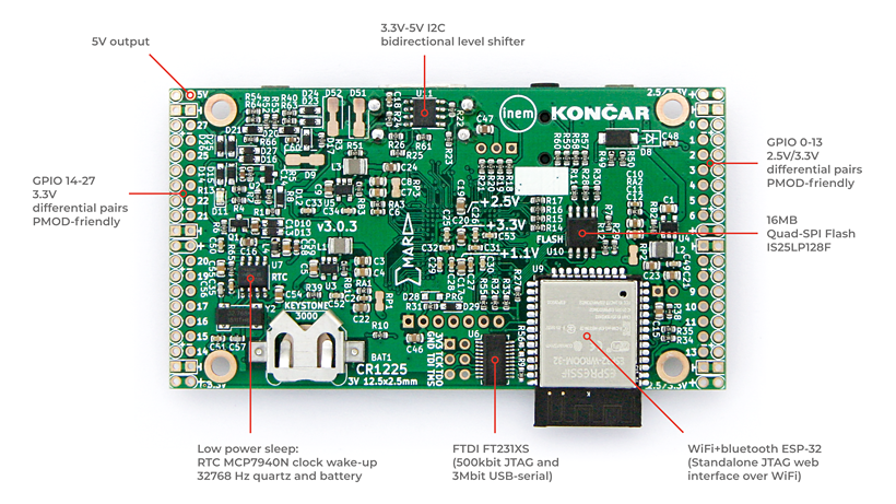
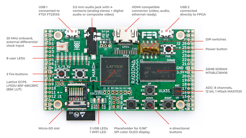
The ULX3S was developed primarily as an educational tool for undergraduate-level digital logic classes. As such, it falls into the “kitchen sink” category of FPGA boards, which include a comprehensive suite of peripherals and devices for development, as opposed to more bare-bones FPGA breakouts. The board includes 32 MB SDRAM, WiFi via an ESP-32 (supporting over-the-air update), a connector for an SPI OLED display, USB, HDMI, a microSD slot, eight channels of 12-bit ADC (1 MS/s), a real-time-clock, 56 GPIO pins, six buttons, 11 LEDs, and an onboard antenna for 433 MHz FM/ASK. This seems like a great set of I/Os for both students and anyone else starting FPGA development.
The ULX3S supports members of the Lattice ECP5 FPGA family, ranging from the 12F (12 k LUTs) to the 85F (84 k LUTs). What can you do with this much FPGA horsepower? Have a look at the long list of examples curated in the ULX3S Links repo. There, you’ll find code from retro-computing to retro-gaming, the usual LED and HDMI demos, and even Linux running on a mor1kx OpenRISC core. Maybe the most interesting links in the repo, however, are those that show how to program the FPGA with a completely open-source toolchain. Proprietary toolchains are the last link keeping some vendor’s FPGAs from wider adoption in the OSHW community, and it’s great to see people chipping away at them.
The board itself is completely open-source. In the GitHub repo, you’ll find the KiCAD 5 design files for the PCB released under an MIT-style license. Even more impressive is the advice in the README, which not only welcomes independent production of the boards, but gives some solid advice on dealing with PCBA vendors during manufacture. Our own advice is to do the right thing and offer the developers a cut if you decide to independently market this board, even though you aren’t required to by the license. If want one, but don’t want to manufacture your own, you can contact the developers using the email or gitter links at the bottom of the ULX3S page: they’re currently doing a small production run.
The Radiona Org folks have created a few videos showcasing example code. Check out how the on-board ESP-32 runs a web server that can load bitstreams into the FPGA (in this case for some retro-gaming), after the break.
If you’re new to FPGA development, and not quite sure where to begin, have a look at some of the FPGA tutorials we’ve collected on hackaday.io. Some ULX3S developers have also been known to hang out on our own FPGA chat room, which is a good place to seek advice about all things FPGA.
We’ve covered FPGA development boards before, such as the FleaFPGA Ohm, which also uses an ECP5.
Thanks to [Igor] for the tip!


I have one! They are very nicely designed bits of kit. Being able to program them over wifi is very cool. The documentation and examples are getting there and I hope to do some very cool things with the board very soon!
screen + usb + power
I need https://hackaday.com/2019/01/10/program-this-badge-in-lisp/ but with fpga ;)
and 2 host USB
Isn’t the problem with Ethernet over HDMI is that so few devices use it that it might as well not exist?
We have connected ethernet bidirectional differential lanes
to the right connector pins where they are supposed to be.
Of course we aware that ethernet over HDMI routers, TVs and STBs
don’t exist in every home (if they exist at all :), but the specifications
exists at least on paper.
FPGA board is experimental board so implementing HEC
protocol between two ULX3S boards would be cool challenge
and fruitful hacking experience therefore we provided possibility
for this, regardless of what the consumer mainstream thinks
about such ethernet.
For HDMI, are they paying a royalty? That has kept me away from HDMI in the past but I’m seeing more and more boards with HDMI connectors on them which has me asking…
no royalty required if you use your FPGA to encode decode https://www.fpga4fun.com/HDMI.html
Hi, Its not HDMI it is GPDI (General Purpose Differential Interface), Electrically LVDS, mostly TMDS tolerant female receptacle more-or-less compatible with digital monitors/TVs.
Tnx Jeff!
My comment was on first comment not on yours!
Thanks for the info. Very interesting!
https://twitter.com/fpga_dave/status/1087038462019149831 David managed to get 1080p30
I know the focus of the board is the ECP5. However there appears to be a complete epic fail not routing the ESP32’s JTAG lines to an FTDI chip or a header (at least in rev 1.0). There is a call out note on the schematic, but HSPI is used for SD-CARD instead of VSPI overriding JTAG assignment. You really can’t use the board efficiently for serious development of ESP32 code with no debugger and stuck downloading code at serial bit rates. Though I supposed one could add a BT or WiFi bootloader to reflash the flash app.
Epic minor fail not using the WROVER module with 8MB flash / 8 MB PSRAM.
Other than that…
I carefully designed ULX3S PCB, so trust me, there is no single feature
you can think of that our onboard chips have and ULX3S board didn’t
make use of. Sharing SD card between ESP32 and FPGA in SPI 1MB/s or
MMC 2MB/s mode, seamless and non-brickable flashing of both
ESP32 and FPGA over the same USB port any time you like is no exception.
It is done using “passthru” FPGA bitstream (we have on github source and binary)
which can even autodetect ESP32 programming protocol and automagically
re-route usb-serial traffic to the right destination.
Try it, plug ULX3S, select in ESP32-arduino any similar board like
“ESP32 WEMOS LOLIN32”, open “blink” example, click upload and you
should see blue LED blinking, change your code, upload, it will work
again. JTAG the FPGA over the same USB port, it will work also.
ESP32 WROVER is too big to waste precious PCB space, even more so
because WROOM’s with 8MB and 16MB flash will be soon available.
Hop that’s good enough for normal development so you can relax and
focus on your code.
Emard answer is on moderate review, so here is his thinking…
Emard carefully designed ULX3S PCB, so trust him, there is no single feature
you can think of that our onboard chips have and ULX3S board didn’t
make use of. Sharing SD card between ESP32 and FPGA in SPI 1MB/s or
MMC 2MB/s mode, seamless and non-brickable flashing of both
ESP32 and FPGA over the same USB port any time you like is no exception.
It is done using “passthru” FPGA bitstream (we have on github source and binary)
which can even autodetect ESP32 programming protocol and automagically
re-route usb-serial traffic to the right destination.
Try it, plug ULX3S, select in ESP32-arduino any similar board like
“ESP32 WEMOS LOLIN32”, open “blink” example, click upload and you
should see blue LED blinking, change your code, upload, it will work
again. JTAG the FPGA over the same USB port, it will work also.
ESP32 WROVER is too big to waste precious PCB space, even more so
because WROOM’s with 8MB and 16MB flash will be soon available.
Hop that’s good enough for normal development so you can relax and
focus on your code.
This thing is pretty cool. The FPGA on it has a lot more LUTs than the FleaOhm does too. I hope it can be made more available at some point. I’d love to see it built into something like an ELLO 2M form factor. Especially if the FPGA can be setup with some classic computing cores and the ESP32 can be programmed for wifi/bt connectivity for it.
I want one….
I saw these in the flesh at 35C3 — [Tobias], one of our assembly members, was an early backer of the project and had a board. It’s very cool that it’s got all the resources onboard to make a full Amiga copy, for instance, but the board really shines as an everything-included dev board for learning essentially anything with FPGAs.
The downside is that a) they’re not in full production b/c it’s a hackerspace project and the college students who needed the boards for class had first dibs and b) they’re probably going to be a bit pricey just b/c they have everything included already.
But how cool is a board with JTAG over WiFi and tons of memory and connectivity? Very cool.
I’m hoping that with interest more boards will be made, I have one and will probably get another…I’d much rather support a hackerspace in Zagreb than Xilinx or Altera. The open source software side of things is too much to pass up!
Whoever plans to experiment with some of the fairly common things like video/audio, low-power, retro gaming/computing, radio, logging, etc. might find that this concept is actually cheaper than buying ton of separate PMODs or whatever… And you end up with much cleaner and compact project, letting you use pins and time for the creative part.
ULX3S looks like very well balanced and thought-out dev board. Definitely not some kind of everything-randomly-included A4 sized expensive nonsense.
There may still be a few lower-end boards that college students didn’t grab available @ around 55 EUR + VAT, (depending on FPGA size – ECP-12F or 25F): http://skriptarnica.hr/vijest.aspx?newsID=1466 … try pinging them at skriptarnica@skriptarnica.hr
My my similar project, also contains ESP32+FPGA – https://hackaday.io/project/159392-prj65-67-esp32fpga
Great board, tnx for sharing! So do you “flash” FPGA with ESP32? And if so what code are you using for that?
Cool board! Interesting choice is CAN bus for car control or similar
electro-noisy applications.
For WIFI flashing, ULX3S boards use https://github.com/emard/LibXSVF-ESP.
With small adaptation (display, buffer-friendly SVF) maybe this Altera-based
board would also be flashed.
If you want to make one yourself the most useful link is probably the Kitspace page: https://kitspace.org/boards/github.com/emard/ulx3s/
Very nice board. I just wonder if the HDMI connector can be used for HDMI input (Rx) as well. Dou you know if this is possible? Is there reference design available?