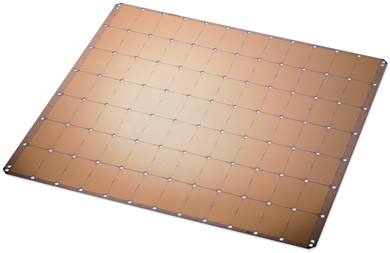
We get it, press releases are full of hyperbole. Cerebras recently announced they’ve built the largest chip ever. The chip has 400,000 cores and contains 1.2 trillion transistors on a die over 46,000 square mm in area. That’s roughly the same as a square about 8.5 inches on each side. But honestly, the WSE — Wafer Scale Engine — is just most of a wafer not cut up. Typically a wafer will have lots of copies of a device on it and it gets split into pieces.
According to the company, the WSE is 56 times larger than the largest GPU on the market. The chip boasts 18 gigabytes of storage spread around the massive die. The problem isn’t making such a beast — although a normal wafer is allowed to have a certain number of bad spots. The real problems come through things such as interconnections and thermal management.
The white paper is detailed while still managing to be a bit fuzzy. In addition to somehow solving the interconnect, packaging and thermal problems with using a whole wafer, the architecture of the cores is supposed to be amenable to sparse matrices and the specific types of algorithms necessary for deep learning.
There’s no word as yet on cost or specific availability, but we were hoping at least for an emulator. However, it is certainly big and if it lives up to its promise could drive new deep learning applications. We’ve seen neural network coprocessors before. We even had our own deep dive into them.


Also pulls something like 15kw
I wonder if they string the cores to reduce power. String 12 cores with a 1V drop each and supply 12V to the wafer at 1/12th the current. That’s what Bitmain does with their Antminer boards to make the power management circuit more manageable.
I can’t imagine this wafer running off 1 or 2V, since that would mean a power supply in the range of 1000 Amps.
The chip will be used decrypt Russian BK47 military cipher and 10,000 AES-CTR 256-bit key decryptions a second.
“According to the company, the WSE is 56 times larger than the largest GPU on the market. ”
And no computer it’ll fit in. ;-)
“However, it is certainly big and if it lives up to its promise could drive new deep learning applications. ”
If it solves the problems you mentioned, more than just DL will benefit.
You don’t fit it in a computer. You fit the computer in it!
Why not? You can fit a computer into FPGA. And maybe there is a few of computers (cpu+memory+…) in the chip.
That’s one core per pixel on a VGA display – with 100,000 cores to spare for calculations! *demoscener drooling*
Judging by Alexander’s comment at the very bottom, that just may be a viable joke. The constant push with ever faster PCIe speeds may make that viable.
So they used a whole 300mm wafer and put 84 550 mm^2 dice on it, using only two thirds of the available space. I wonder why they didn’t bother to use the whole wafer: they could have easily fit at least another 16 dice on it to make a nice round 100. (max number that can fit is ~112)
Maybe they had an old ATX case they wanted it to fit.
And wow, I wonder what their yield was… Online die yield calculators suggest it’s an iffy proposition.
My theory is they actually have more cores than they are claiming and that is how they are getting around the yield problems. That way when some fail to work they can mark it as such in some on-chip configuration storage chip and still operate properly.
Agreed. And I think that’s why you also get MCUs in two flash sizes. When they start production they can try to build the bigger one and all dies that fail less than half the flash get sold as the smaller one. As yield goes up, you start marking good chips as the smaller ones, and that’s when you start actually producing the smaller die with less flash.
Sometime they won’t even bother making a specific die for the smaller size as it would cost them more money for the layout/verification/new mask/separate batch than the extra die size.
Chip tester is a bottle neck on the production line. They would only bother testing 1/2 of memory to save time on the tester.
> all dies that fail less than half the flash get sold as the smaller one.
Memory is one of the easiest thing for them to improve yield simply by having a very small percentage of “spare” rows for redundancy. If there is a defect, they simply swap it out. The memory is a small portion of the die, so they would have to drastically redo the layout before they can reclaim the space.
What they are actually doing with the two memory sizes and sometimes peripherals is called price discrimination. https://en.wikipedia.org/wiki/Price_discrimination
It gives their customers a warm and fuzzy feeling that they have somewhere to go for upgrade.
e.g. STM32F100 (without USB) is actually STM32F103 (USB) and they are used in Chinese STLink clones instead of the F103 part. The actual Flash sizer of both parts are their bigger bothers at 128kB instead of 64kB. For accounting reasons, they are actually saving money not having to do 2 layouts, mask, production runs by sharing the same dies.
The perimeter of the wafer often as much lower yield than the center. They might have had to limit the size, to ensure a reasonable yield.
If I can cool it with waffle batter it’ll be a great personal assistant! I come up with the greatest ideas while eating waffles!
If [richter]’s 15 kW power figure is correct, you could have pretty good waffle throughput too! (though I don’t think silicon carbide wafers come that big, so it’s likely the regular stuff and can’t get hot enough for waffles and still function.)
My initial estimate was that the 15kW was “way too much”. But if we assume a normal CPU is about 1 cm^2 and consumes about 100W. This is about 400 cm^2 so that would come to 40kW! Because you can’t fit a CPU cooler on each square cm in this thing, a lower power/area figure makes sense. 15kW is realistic.
Getting 15kW at about 1V into this thing is… tricky. Getting the 15kW of heat out is… tricky.
Why can’t you fit a cooler on each square cm?
Of course you would bolt this monster to one big cooler. liquid cooled of course. 15kW makes a nice on-demand water heater. You could operate a public shower bath with it :-)
I think, the bigger problem is, to deliver 15kA of current. We have to take a look at the big power thyristors (SCRs): Sandwich it between two of this cooler copper plates, one GND, one +1V with some tons of clamping pressure. These parts also take several kA and switch up to several kV, with about 1V or 2V as residual voltage if switched on. So you have to take away several kW of heat. The unit I saw years ago was only in the 1kA/1kV range and had massive heatsinks, a 50cm long squirrel cage fan and it’s motor alone was a 3 phase motor with 100W or 200W.
Presumably they fill the bottom of the PCB with converters and use a high voltage to distribute power, so the current density at any point shouldn’t be too bad. Going to need quite a big pump and radiator for the water cooler, but nothing exotic either.
It is going to be messy to get a low DC loss as well as low high frequency AC impedance (decoupling) for the cores.
The regular PCB copper thickness might not be sufficient to handle the high current. Regular 1oz copper has a sheet resistance of 0.005 ohms per square. You are looking at 10,000A range, so that won’t cut it. You can only go so far (4oz) and with multiple layers.
Vias make Swiss cheese out of power/ground plane, so I am afraid that the center part of the chip would suffer a lot.
Now that’s an idea, put the thing/cpu/wafer with suitable comms eg ultra wideband wifi/Poe etc make it a fryer/waffle iron and both sides too, then each time you feel like cooking waffles or heat McNuggets left overs etc you can run any number of programs from Bitcoin mining to protein folding solutions to Seti pattern/fft to mapping game play to searching for patterns in any data sets eg stock market ;-) to movie rendering your storyboard creations – so as not to feel you are just wasting that heat – do something ‘useful’…
Of course if you do get attached to it’s immense power and utility then your other half might raise more complaints leading up to meal times now trashed “What the heck, what is it with you and waffles, that’s the fourth time today in just the last hour ! ” – so what she can just dry her hair more and have the washers on hot more often every one wins :-)
Seriously wouldn’t it be interesting that any electrical source applied for heating could instead be a processing module by default for any number of uses with heat then as the side effect byproduct and which happens to be most useful in winter, even viable in summer air con as thermal pumps eh heat driven refrigeration (Einstein fridge) – nice way to turn tables on values of those electrons, this could well be a developing trend if at least low density heating until semiconductor tech eg advances in Silicon Carbide etc to handle higher temps :-)
Thanks for post, keen to look at processor architecture and inter processor comms, cheers
Yes, like, what if every lightbulb was also an infrared radiating heater. Twice the value for the electricity.
Wouldn’t that be something.
Reminds me of the story of the an office building in Toronto: they were told to turn off the lights at night to save money… but the waste heat they generated kept the building from freezing at night and needed to be made up by using the natural gas-fired heaters. Turns out that the nighttime rate for electricity at that scale is near zero and, being essentially 100% nuclear-sourced at that time of day, also produced no carbon. So the myopic bean counters making the lights-off demand ended up paying more AND increasing the carbon footprint. (though I’m sure relamping cost didn’t figure into the popular-press version of this).
Highest stress for bulbs is the on cycle, followed by the off cycle, steady state(eg being left on all the time) is actually the best for longevity. There may be something about burning up the phosphor coating on newer bulbs, but afaik that’s usually not a concern (other parts wear out much faster).
Years ago on a ballance scale company everything was mechanical. To optimise performance the lab had to be kept to exactly the same temperature, it was well insulated, and had a filament light bulb for each worker. When they left the lab , they had to first turn on their globe, it is set to the same amount of body heat they give off on average. That way they could prevent the thermal shock of an individual entering or leaving the lab.
So, are we in agreement? Can I have my super smart waffle iron? Seti at Home won’t let me contribute from all my old P4s anymore, and I have to have an extra reason to stoke those coals anymore. And since they’re all single die, I have to piece together a bunch of sub-waffles to make one.
‘led blinking intensifies’
If this pans out, what can it emulate? The current most powerful super computer at full speed? Or even Crysis at max setting?
Dodgy back of napkin math: they claim 46,225 mm^2 is 56x the largest GPU, so that’s 825 mm^2 – close enough to the 815 mm^2 Nvidia Volta V100 for me to use as a comparison – used in the Titan V with some stuff disabled, and the Quadro GV100 fully-enabled.
So then, assuming power output scales with area linearly and they’re running at the same clocks (I dunno, I’m just making this up) power output is less than the TDP of 250 W x 56 = 14,000 W, as a reasonable power ceiling. I think I’d try to cool it with a big-ass waterblock with lots of channels.
A supercomputer with 16 GV100s costs $400,000 so if performance per watt is the same and they’re charging the same, you’re looking at a cool $1.4m for one of these.
But will it run DOOM?
It’ll run every possible permutation of doom.
It goes back to my idea of how many zx spectrums can you fit on an i7 die and takes it to the next level. I’m guessing they must shut down cores periodically to allow cool down time and the holes allow coolant to pass through the chip.
Now stack together 20 and you’ve got your first real brain on a chip.
But will it run Quake?
Для тех, кто понимает и помнит КВН 80-х:
В СССР выпущена самая большая интегральная схема в мире. С 80 ножками и двумя ручками. Для переноски.
Sorry, guys, word play in Russian – it’s hard to translate.
Now a smaller commercial product in the offering but, only 35 billion transistors, dear oh dear, size matters sob sob…
https://amp.tomshardware.com/news/xilinx-world-largest-fpga,40212.html
Is that how you justify theft?
That’s one core per pixel on a VGA display – with 100,000 cores to spare for calculations! *demoscener drooling*
cores, who cares? lets make a decent ccd for large format photography :)
Just… don’t… drop it!
or even look at it harshly. I dropped a 4-inch wafer once. For something so light it’s distressing how many pieces it becomes.
A myriad razor sharp, eye-wateringly expensive pieces.
I have a $2,000 300mm wafer pinned to the wall of my cubicle. I use the back side of it as a mirror.
Pretty neat what a refractive index of 4 will do, isn’t it?
Next neat trick: look through it with an IR camera. It becomes transparent around 1000 nm, right about where CCDs start to poop out (not surprisingly, if you think about it). You can easily see incandescent-lit scenes through it.
Moore’s Law makes my head spin. All that switching and current needed to go through all those gates…it just…words cannot explain.
Just to be quick.
Making Wafer Scale Integration is honestly fairly easy. (The larger interconnect layers can just poke out the side of a “chip” into the next “chip”, then one simply doesn’t dice up the finished wafer, this would though leave a very obvious grid pattern. (As can be seen in the image.))
Getting around yield is also easy. (This can be done by routing the bus resources in software, thereby avoiding both broken cores, memory, and even bus controllers. This means that broken parts can be disabled and thereby not effect yield.)
Supplying sufficient power. (On chip buck converters aren’t a new thing. But one can also just stack one set of logic on top of another, in terms of voltage. This though means we need to AC couple our signals between the voltage layers. (Stacking core voltages can though need silicone on insulator technology, but this is fairly common to start with.) Then there is the fact that the WSI chip is gigantic, there is plenty of space for power pins.)
Big downside is connecting the chip to a PCB…. (BGA yield is largely proportional to pin pitch and array size. Then there is thermal expansion to take into consideration.)
Cooling this beast of a chip is though not hard. (LN2 is cheap (A thick copper/metal block between chip and LN2 can be needed to avoid cold bugs, if this is a problem that is.), then there is also water cooling. Both of these tend to handle high thermal densities rather efficiently.)
In the end, the bigger question is, is this worth the trouble?
The answer can simply be summed up with: “It depends.”
The main advantages of WSI isn’t large core counts, nor huge amounts of integrated memory, these are still attractions, but one can just use multiple chips spread out over a PCB for easier power delivery and cooling. So for just cores and memory WSI isn’t a needed solution.
But the fact that building buses on a chip is trivial, this means that if you want a 8192 bit wide buss between two points, running at 2-16 GHz, then no problem, just build it. If you have the transistors to drive and buffer it, and sufficient switching speed, then you have most of what you need, other then routing space. Additional interconnect layers do cost money, but even a dirt cheap 1µm node can place around 500 traces for every mm of width. (Most PCB manufacturers would struggle to place more then 10 traces per mm.)
This means that if you need a lot of cores/memory, and a lot of bandwidth between them (and likely low latency), then WSI has a more alluring offer then individual chips on a PCB.
It took approximately 10 years to develop this:
https://flagship.kip.uni-heidelberg.de/public/BrainScaleS/index.html
Working interconnection was the hardest part afak.
Does it come in a DIP package for easy prototyping?
So does it work?
A company called Trilogy systems tried to do something similar back in the 1980s
https://en.wikipedia.org/wiki/Wafer-scale_integration