One of the great things about the Arduino environment is that it covers a wide variety of hardware with a common interface. Importantly, this isn’t just about language, but also about abstracting away the gory details of the underlying silicon. The problem is, of course, that someone has to decode often cryptic datasheets to write that interface layer in the first place. In a recent blog post on omzlo.com, [Alain] explains how they found a bug in the Arduino SAMD21 analogRead() code which causes the output to be offset by between 25 mV and 57 mV. For a 12-bit ADC operating with a reference of 3.3 V, this represents a whopping error of up to 70 least-significant-bits!
While developing a shield that interfaces to 24 V systems, the development team noticed that the ADC readings on a SAMD21-based board were off by a consistent 35 mV; expanding their tests to a number of different analog pins and SAMD21 boards, they saw offsets between 25 mV and 57 mV. It seems like this offset was a known issue; Arduino actually provides code to calibrate the ADC on SAMD boards, which will “fix” the problem with software gain and offset factors, although this can reduce the range of the ADC slightly. Still, having to correct for this level of error on a microcontroller ADC in 2019 — or even 2015 when the code was written — seems really wrong.
After writing their own ADC read routine that produced errors of only between 1 mV and 5 mV (1 to 6 LSB), the team turned their attention to the Arduino code. That code disables the ADC between measurements, and when it is re-enabled for each measurement, the first result needs to be discarded. It turns out that the Arduino code doesn’t wait for the first, garbage, result to finish before starting the next one. That is enough to cause the observed offset issue.
It seems odd to us that such a bug would go unnoticed for so long, but we’ve all seen stranger things happen. There are instructions on the blog page on how to quickly test this bug. We didn’t have a SAMD21-based Arduino available for testing before press time, but if you’ve got one handy and can replicate these experiments to verify the results, definitely let us know in the comments section below.
If you don’t have an Arduino board with a SAMD21 uC, you can find out more about them here.


“For a 12-bit ADC operating with a reference of 3.3 V, this represents a whopping error of up to 70 least-significant-bits!”
WTF? An error of up to 70, yes. How you can have 70 LSbs incorrect in a 12 bit signal, I’m not sure.
Standard terminology: 70 times the value of the lsb.
So, 70x the resolution, or grain.
Not exactly. In a 12 bit adc, that mean you have 4096 “levels”. The adc error, which in this case is now 70 bits, means you have a percent error of 3.4%. (70/4096 x 2) in a 12V system, thats an arror of 0.41 volts.
Not really awful, as it can be used for 90% of all scenarios. But compared to the new 0.035V error thats a big change.
I prefer stating raw ADC readings as ‘counts’. So, the amount of error is 70 counts out of 4096.
This issue with this terminology is that often people pad the output with zeros at the end of the number (ie, for a 12 bit dac, the result might be a 16 bit number that ranges from 65535, but you only get values that are multiples of 16. ie 0,15,31,47,63, etc). Since what you actually care about is the smallest resolvable change in output, the lsb terminology is more accurate and less open to interpretation.
I translated that as: a count of 64 is 2^6.
So an error of 70 means the 6 LSB are bad, with some error creeping into the 7th bit.
You can only “trust” the 5 MSB of a 12-bit reading.
”For a 12-bit ADC operating with a reference of 3.3 V, this represents a whopping error of up to 70 least-significant-bits!”
An error of 70bits in a 12 bit number seems very wrong, am i misunderstanding something?
@dmcbeing: “whopping error of up to 70 least-significant-bits!”, “least-significant-bits” been key here to make sense of that sentence! :)
A least-significant bit can be understood as the smallest value that number can represent (if only the lowest bit is 1).
12-bit number => 4096 possible values;
3.3 V DC / 4096 => 0.0008056640625 V increments or ~0.8056640625 mV
57 mV / 0.8056640625 mV => ~70.7490 or about up-to 70 least-significant bits of error.
“70 least significant bits” means an offset of 70 in the raw value. Think of it as subtracting the LSB 70 times sequentially, not the lowest 70 bits.
Great explanation!
+1
This should be 70 counts, not 70 “least significant bits.”
Thanks…. this makes much more sense
Still the “error is X lsb” is standard terminology.
But LSB is least significant bit, not bits, I think the plural of bit here is what’s most confusing.
The term being standard doesn’t mean it’s a good choice of term.
No, it really is not “standard” it is simply wrong. An ADC may be quoted as having an error of 1LSB, which the last bit may not be relied upon. The fact that that LSB corresponds to one quanta, does not mean that 2LSB is two quanta!
If you confuse bit offset with quanta offset in this way, an error of say 4LSB would be entirely ambiguous. It is only clear what is meant in this context, because the value is so implausible if read taken as read.
If it makes you feel any better, I had the same question on this one and asked Ted to double-check before publication. He came up with the exact same math as rbscharette.
It’s just one of those confusing units of measure, but it is correct in the article.
Shame he didn’t expand the article to include that detail!
This isn’t correct. (But I don’t often see corrections when I post them, maybe I’m wrong all the time…)
This should be 70 counts, not 70 “least significant bits.”
I have seen it being expressed either way, but “counts” would be less confusing. Digital meters are sometimes specified as +/- 1 LSB or +/- 2 LSB, etc.
Meter precision is expressed in terms of least significant digits (decimal) rather than bits (binary), and you will never see anything greater than +/-1 digit in any spec – otherwise that last digit need not be there at all. The term in that context refers to a different measure than the offset described in this article.
It is a bit of a mess, isn’t it? You can assert that “70 least significant bits” implies 70 x the value of 1 LSB. But if you say “the 70 least significant bits” it means the lowest 70 bits of a bigger binary value. One might think it deserves more clarity.
“Counts” is good. And given the degree to which HaD readers like to examine problems, differential and integral non-linearity could help whenever trying to spec an ADC.
I think the article is confusing bits in the ADC with absolute values. An ideal 12-bit ADC at 3.3 Vref would have 806uV per digit. So in this case they mean about 70 raw digit values in terms of error.
For example reading 1000 would mean 0.805V ideally vs reading 1070 which would be 0.862V or offset about 57mV.
TI has a nice application report entitled “Understanding Data Converters” which explains the usage of LSB as a unit (see section 2.1). It’s just somewhat confusing industry-standard notation.
I didn’t make it up :-)
http://www.ti.com/lit/an/slaa013/slaa013.pdf
I’ll defer to your reference vs my anecodes, but for what it’s worth I have never heard this in industry with large offsets like this. I only hear this in reference to things like hardware uncertainty, and even then never with values even an order of magnitude less than what you specify. I’ve never heard this term used this way due to errors from code defect.
Note that the AN you posted stays in the range near 1LSB =)
Always willing to see exceptions.
70 bit error in 12-bit ADC? Sounds wrong.
Maybe it should have been worded as an “error of +/- 70 to the ADC readout”?
That doesn’t look right either…
maybe “a range of 70 counts in the LSB read”?
I would not even call it an error if it is a value from incorrectly using the ADC.
Well, at least it seems to be somehting that a couple of asm instructions in the library can fix.
It’s not that unusual to have ADC offsets. Sometimes vendor code hides it (PSoC), sometimes it’s in full view of everyone (ESP32). Sometimes you just have to do something tricky like running the internal Vref in there so you’re at least as good as that. I’ve also done things like shorting the inputs together if the ADC is differential, anything other than zero is the offset. Even better is compensating for temperature drift. CMOS is somewhat terrible for analog but we deal with it because it’s so cheap to make!
“It seems odd to us that such a bug would go unnoticed for so long”
I guess there are a lot of copy/paste programming amongst arduino users. As long as a library and it’s example code seem to work we are happy. If it doesn’t we can always fix it with a few lines of ugly code. I’m guilty of this sometimes since I started using arduinos to save time in my projects. Before, when writing code directly for the avr, I read datasheets and developed my own code, checked its functionality, debuged, etc…
Dammit! This was not intended as a reply!
The problem is that the SAMD21 is somewhat complicated to program if you’re not using the Arduino libraries, so most people save themselves the pain and deal with the devil they know.
When I was trying to get around the thing, all the other available examples were with ASF, which is a monstrosity. It was very difficult to find any information about how to access the hardware directly like with the smaller AVR chips. It exists, but it’s… complicated…
All the features of the chip, such as hardware timer/counters and pin IO, are “peripherials” that sit on a shared “external” bus to the actual CPU, except some hardware which is also accessible through a dedicated bus, so low level access to the stuff gets weird really quickly. You have to slaughter a chicken and sing a chant to get the data synchronized between the peripherials and the CPU, so that your processor actually gets the value you want to read off of your counter or your pin.
For example, I was trying to use a counter to count the number of pulses coming in through a pin. Everything worked fine, except for the fact that the number in the register did not update until I put the entire chip to sleep, woke it up, and then started the counter again, after which it would update the register with the -previously- measured value from before when the chip was put to sleep.
Also, if you’re bitbanging stuff: realize that because of the internal bus setup, it takes many clock cycles to get the pin IO data from the actual pin to the CPU and vice versa, which in practice means that a 48 MHz SAMD21 is no faster at dealing with IO than a 16 MHz ATmega – unless there’s some trick that I’m missing, but that just goes back to the first point…
“The problem is that the SAMD21 is somewhat complicated to program if you’re not using the Arduino libraries, so most people save themselves the pain and deal with the devil they know.”
All the newer super-micros are like this. The ARM M7 in the new teensy has thousands of pages of docs, and it’s all poorly-ordered gobbledygook.
I guess companies just decide to throw as many IPs on a die as possible and if they sell it cheap enough, a community will develop and people will figure it out.
The problem is that the pre-built libraries will almost invariably have a bug or limitation in the way in which you’re intending to use them, so you eventually need to dig deep and rewrite them anyway. If the app is timing critical, by the time you fix all the jitter, dma, and interrupt issues, you may wonder if you should’ve just started with an fpga in the first place.
As long as the communities don’t complain about this, it will only get worse. Yes, you can get very powerful systems now for a couple dollars, but you might have to buy a $100 in books and/or videos to get a real handle on the internals. Not to mention the investment in time.
These uC usually have very powerful peripherals for real word industrial applications. It is very hard to count cycles for pipeline (and sometime some cached/accelerated FLASH access) CPU cores. if you feel the need to bitbanging an Arm uC, you are likely picking the wrong path or wrong series. e.g. your SAMD chips have very powerful DMA engines that can be abuse to do a lot of things.
For any modern high speed circuits, they have to synchronize signals across clock domains. You’ll also see that on Atmega timers, GPIO by may be a couple of cycles. Arm chips sometimes have more complicated peripherals that can run at limited or specific speeds. e.g. USB at 48MHz or complex timers that don’t run at full processor speeds. Remember that some higher end parts can run at hundreds of MHz. So they have multiple clock domains to cross. Also sometime you use lower clock frequencies to reduce power.
You also don’t exactly want to drive GPIO at full bus speeds as they require very high rise/fall time which can cause EMC and signal integrity issues. There are GPIO slew rate control options at least for the STM32F chips I use: 2MHz, 10MHz,50MHz. May be you didn’t read the user manual?
I don’t know about you, but I didn’t need to watch video/buy books to learn about Arm chips. I did spent 2-3 weeks learning compiling/debugging/porting complex code. After that point, I have picked up more than half a dozen different families and a couple of vendors just by reading the user manual.
Some of us have been around for decades with this stuff and seen documentation and app notes go from immediately useful to garbage. They had to be good, because there were no forums to go to. It’s not like the rest of us have not put in the time and experimentation, either. You are just obviously superior to many of us in this respect.
@Luke on not reading values from peripherals.
May want to check if you have variables that deals with peripheral need to be declared as volatile. Arm compilers can be very good at keeping variables or expressions across lines of code and sometime they would optimize them away not knowing that they can be modified by IRQ, DMA etc.
That or there are certain preconditions that you have to follow. e.g. some peripherals do not like their parameters change while they are running. They have to be disabled, change values and then re-enable again.
The root cause of the error was a common mistake — reading a value from the ADC before it’s ready. This is definitely one of those classic “read the datasheet more carefully” mistakes, and it’s one that I’ve made too.
Between the front-end multiplexer and the sample-and-hold capacitor, there’s all manner of free-room for mischief.
“It seems odd to us that such a bug would go unnoticed for so long […]”
“The root cause of the error was a common mistake — reading a value from the ADC before it’s ready. This is definitely one of those classic “read the datasheet more carefully” mistakes, and it’s one that I’ve made too.”
I feel like that hits on why it probably was not figured out sooner: the Arduino platform/environment is aimed at people who are told to not look under the hood, so to speak (i.e.: get results quickly with embedded stuff without dealing with the complexity of embedded stuff). Therefore, we shouldn’t be surprised when they don’t and such subtle issues stay hidden for a long time.
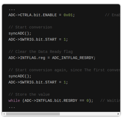
“That code disables the ADC between measurements, and when it is re-enabled for each measurement, the first result needs to be discarded. It turns out that the Arduino code doesn’t wait for the first, garbage, result to finish before starting the next one.”
Oh boy…BTDT with lab equipment I’ve built. This is a tough lesson and in my (amateur) opinion, it should be “toss the first value as a matter of course, unless there’s a good reason not to”.
So…
would NOT disabling the ADC between measurements fix this?
Or is the power used by leaving the ADC on a bigger problem?
@Ren: Would probably be simpler if it was never disabled between readings… but that wouldn’t play nice (*assumption*) with other stuff that could be running that expect those resources to be free between uses of analogRead(), such as other libraries (possibly?). I feel there’s no easy way out of this when you want appeal to people who are not interested in the deeper workings of the components (such as peripherals, SFRs, interrupts, etc.).
The Arduino libraries seem to (mostly) return things to a known state after doing something. By leaving the ADC on after measurements, you’d be creating a situation where you’re toggling things on and off without an explicit way of knowing what the state of the system is.
In other words, to change how it works, you’d have to create a new function that enables the ADC, then another that reads it, and then a third that disables the ADC. That would confuse all the Arduino users, who are accustomed to just using one function.
+1
“In other words, to change how it works, you’d have to create a new function that enables the ADC, then another that reads it, and then a third that disables the ADC.”
That kinda sounds like an asynchronous library for the ADC… :D
Something like this would make sense in a system with DMA, which most µC used for Arduino platforms don’t seem to have, at least on the lower end.
Technically speaking, with most chips supported by the Arduino libraries, the ADC works by first setting up the correct registers to set the parameters, then you trigger the conversion by writing to some register, then you wait for the conversion flag, then you read the registers, then you do whatever you want – and then you set the registers again to turn the ADC off if you’re going to sleep or doing something else with the pin.
The Arduino libraries do that for you. The disadvantage is that you could be running code while the conversion is taking place, but in most cases you’re just waiting for the ADC value anyhow.
There is a much deeper concern for the amount of peer review/code testing for something that have a huge noob user base. The “many eyes” do not know what they are supposed to see.
The platforms for noobs built by noobs and what can possibly go wrong? “I am not just the CEO, but I am a client too”.
I’m surprised that the terminology causes confusion amongst those who actually use microcontrollers – if you don’t understand or disagree then you should probably read up on the basics on ADCs. But I can see the confusion with those who perhaps aren’t regular uC users. A least significant bit is the smallest step in quantization, the plural meaning the number of these steps, not how many binary digits. I rarely use “count” since this harks back specific ADC architectures.
The muddy the water further, when deal with words, 16 or 32-bit, the LSbyte and MSbyte do indeed refer to the placeholder location rather than absolute value.
You can’t expect much from a crowd whose understanding is that a PWM waveform is “analog write”.
Given with a spoon, can’t be demanded with a ladle.
I’m a tinkerer and no expert but I guessed that the 70 lsb’s was referring to the read value. So if it should be reading 100 it would incorrectly return 170 to the program.
Am I right?
Yes, if you mean the raw binary values (no scaling). Like 1000110 and 10101010.
The Arduino code linked from Omzlo (https://github.com/arduino/ArduinoCore-samd/blob/master/cores/arduino/wiring_analog.c) does not touch the ADC->CALIB register at all, and that’s plain wrong. You need to write factory-calibration values from the NVM controller to the ADC->CALIB register to make the SAMD21 return sane ADC values.
Quoting the datasheet: “33.5.10 Calibration The BIAS and LINEARITY calibration values from the production test must be loaded from the NVM Software Calibration Area into the ADC Calibration register (CALIB) by software to achieve specified accuracy.”
I believe they do correctly load the calibration data at initialisation in https://github.com/arduino/ArduinoCore-samd/blob/master/cores/arduino/startup.c (see line 286 at after)
The code shown in the blog focusses on the measurement part (https://github.com/arduino/ArduinoCore-samd/blob/master/cores/arduino/wiring_analog.c).
I think it was meant to be ~ 6.129 lsb or log2(70)
I wonder if the similar error of the ESP32 A/D converter is due to a similar problem with the Arduino libraries?
We could expand the discussion to specific areas in the ADC that contribute to the fail but likely way overkill. As an analog designer I understand how this can occur. I believe it comes down to the cost of test. If the SAMD21 had a limited number of pins that could be used for analog functions then it’s fairly easy to trim out INL/DNL type errors. But when you have a huge number of potential input paths and combinations then the test time can grow huge and more important the trim memory size becomes rather large. I think the manufacturer made a trade off and when combined with poor software we get this. After all a micro controller with an ARM core and a set of peripherals is just dirt cheap in today’s market. Trimming out cost at the expense of analog trim is likely the inevitable outcome.
Noted the ADC err “back in the day” and muttered something inappropriate for here. Wrote code to determine the offset and gain needed for each channel and applied those values with a subroutine in my target code. Solved.
Need for ADC zero and gain adjustments has been with us since the start, and due to tiny variances in manufacturing will be with us forever.
If you need high accuracy across the full span of readings you can also add code to compensate for “curve” of the slope so the full range of readings is accurate rather than just those near the points of zero and full scale.
Though imperfect as manufactured, to build corrections into the chip would have driven the cost up quite bit at a time everyone was competing based on cost per unit.
Makes me wonder how accurate the readings are from the ADC of any of these type of boards going forward.
I’ve worried about and spent not an inconsiderable amount of time checking the accuracy of reference voltages and money buying quality (for an arduino anyway) reference devices but never considered that errors in ADC reads would have such an impact.
Thanks for the heads-up.
I’m amazed at some of the naivety of many of the comments that are interspersed with good, solid engineering comments. This results in a lot of noise (needs better curation). I just went through ALL the comments (at least, those that existed when I started reading), AND NOT A SINGLE ONE REALLY BLAMED LACK OF TESTING AS ONE OF THE BIGGEST FAULTS. There are lots of variations in ADC architectures (SAR, sigma-delta, dual-slope and variants, flash, …) and most, if not all, micros use SAR which adds one bit per ADC clock cycle (so, a 12 bit ADC needs 12 clocks). The various comments on “counts” is more appropriate for dual-slope type converters that use “about” one clock per quanta (these also have bowed transfer curves if there is too much dielectric absorption in their integration capacitors), but they also have a “zero” cycle counts not seen by the user, and more “mystery”. sigma-delta ADCs run a some multiple of their effective bit conversion rate and achieve accuracy/resolution by LP filtering the lower frequency noise out.
Back in 1989, I tried to use an Intel 80C196 processor’s 10 bit SAR-based ADC. Trouble was, it had a switched capacitor architecture, not a “normal” R/2R resistor network, and was unbuffered so that it placed a variable capacitive load on whatever it was connected to. So, our engineer who designed the board never buffered those inputs and they were unusable, getting about 4 to 5 bits of resolution! Fortunately, when I specified the external 12 bit ADC input mapping, I routed those signals there too and ended up using a single 12 bit conversion between blocks of 1024 samples of that ADC and that’s how it still runs to this day (OK, so the 80C196 was retired by Intel in the early 2000’s, but we bought 1/4 million units at EOL).
And for those that weren’t able to filter out what an LSB is in the prior discussions: [1] an LSB is the smallest conversion unit (i.e. step or quanta size); [2] it’s based on the number of “bits” in the ADC; and [3] its IDEAL value is (1/2^ADC_bits)*FS, where FS is the full scale range of the ADC. Thus a 10 bit ADC with 5V FS (like in AVR parts running at 5V) has an LSB that’s (1/2^10)*5V or 4.88 mV for a PERFECT, IDEAL step size. Note that no ADC can measure FS — it’s max value is one LSB less than FS (and that’s assumes everything’s perfect).
Also, no one ever discussed slew rate, capture times, settling times, etc., which are all critical to maintain the highest accuracy of an ADC’s conversions. But that’s for you to research.
Some of you, I expect , “are welcome”. From a guy who got his BSEE in 1976.
Notable update: The bug has been corrected by the Arduino team in a recent PR: see https://github.com/arduino/ArduinoCore-samd/pull/447
Hello, Ive noticed another problem with SAMD21,using adafruit Metro M0 express.It doesnt set your samplerate to what you specify. Heres my link: https://forums.adafruit.com/viewtopic.php?f=63&t=161738 ….