Decapsulating ICs used to be an exotic technique. (I should know, I did that professionally for one of the big IC vendors back in the 1980s.) These days, more and more people are learning to take apart ICs for a variety of reasons. If you are interested in doing it yourself, [Juan Carlos Jimenez] has a post you should read about using acid to remove epoxy from ICs.
[Juan Carlos] used several different techniques with varying degrees of success. Keep in mind, that using nitric acid is generally pretty nasty. You need safety equipment and be sure to plan for bad things to happen. Have eyewash ready because once you splash acid in your eye, it is too late to get that together.
We never took apart MEMS devices, so that was especially interesting. A little metal lid keeps the epoxy out of the moving parts and that turns out to be hard to remove.
We were surprised he used 69% nitric. We used to use white fuming nitric, but that may be a bit harder to get now since it is associated with explosives. Then again, you can make it yourself. We used to also use copper bars to sit between the hot plate and the device to get better heat transfer. The acid reaction is much stronger when you heat it.
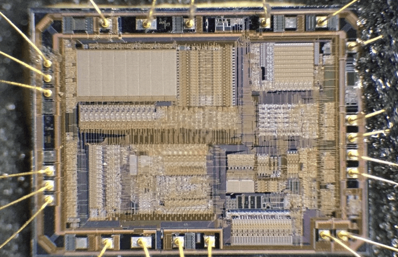
By the way, if you ever wanted to actually probe the device, you’d have to remove the passivation layer which is SiO2 glass. That takes hydrofluoric acid which is very nasty stuff, indeed. You can see the edge of the passivation around the bond pads under a microscope. You’ll notice the surface of the pad focuses differently than the edge where the thin passivation layer starts. When you can’t see that edge anymore, you’ve removed the glass.
Of course, you might not need to probe the actual circuit to get results. If you don’t care about the circuit’s survival, you can try more mechanical means.


Sometimes you can scratch through the passivation with a microprobing needle
There was a talk at the most recent Shmoocon on IC chip decapping on the cheap. Apparently the presenter had success using a blow torch.
https://youtu.be/mriu_O8bhck
Yeah, at work we called it bic decap.
I had a lot of luck with putting the chip on a milling machine and removing most of the encapsulation and then cooking off the bit remaining with a nearby flame. If I had multiple chips to practice on, I could usually mill down to 0.05mm above the die surface on the second try.
I think if I had a bond diagram I could probably manage to mostly avoid the bond wires, too. We didn’t try that.
There are papers on using ethylene glycol to do low temperature (200C) degradation of epoxy, that combined with careful mechanical removal, might end up with a fairly low toxicity, albeit slow, decap, that results in a functional chip.
(For our chips, nitric acid isn’t really a great choice anymore if we need a functional decap since we’re not using gold bondwires anymore.)
Yeah I was working on this in the mid 1980s so a lot has changed since then. For one thing, most of the big chips now are upside down ;)
Presenter at the most recent Shmoocon had an unusual method of chip decapping – using a blowtorch.
https://youtu.be/mriu_O8bhck
I used pure sulphuric acid to decap a chinese chip here: https://smdprutser.nl/blog/decap-a-chinese-chip-at-home-clone-or-not/
Did it outside with lots of precaution. Had gloves and goggles.
Any thoughts on affordable microscoop?
There is no such thing as “pure sulfuric acid”. There is concentrated like 96 %, though.
There were a few times I accidentally did that, by shorting the power to the wrong pin. ;-)
My last one was pausing the debugger… *pop* exposed die on the boost converter MOSFET. ;D
Ah… the memories that magic smoke bring back…
This looks pretty spectacular if you’ve already decapped the die and are looking at it through a thermal camera when you short the power. An unintentional accident while looking for something else
Neither sulfuric nor hydrofluoric acid is stuff i want to mess with. But somewhere on the internet somebody experimented with “cooking” the IC in (melted) colophonium. Sure, you should do this outside and take some precautions, but it seems a lot less dangerous than acid. Did anybody try this?
This guy just uses a hot air gun to decap a few ICs looks simple if you can get your hot air gun up to 500degC: https://www.youtube.com/watch?v=ZQeHHYJYWXo&ab_channel=CuriousMarc
How would you decap on a huge scale chemically? Fuming nitric acid is to expensive and dangerous. So is there another inexpensive way?
There is no huge scale decapping. Even FA labs only work on a few chips per project as this is very manual process. They will usually have a test case used to identify the worst performing chips to make whatever they’re looking for easiest to find and only need a few units.
Beyond failure analysis, extreme investigation of counterfeits and idle interest in seeing the die I’ve never seen another market for decapping IC’s.