Designing your own integrated circuits as a one-person operation from your home workshop sounds like science fiction. But 20 years ago, so did rolling your own circuit boards to host a 600 MHz microcontroller with firmware you wrote yourself. Turns out silicon design isn’t nearly as out of reach as it used to be and Matt Venn shows us the ropes in his Zero to ASIC workshop.
Held during the 2020 Hackaday Remoticon, this is a guided tour of the tools used in the Skywater PDK — the Process Design Kit that is an open-source ASIC toolkit produced in a partnership between Google and SkyWater Technology. We covered the news when first announced back in June, but this the most comprehensive look we’ve seen into the actual design process.
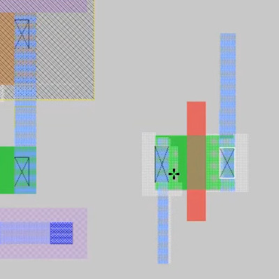
Matt builds up the demo starting from the very simple design of an N-channel MOSFET with click-and-drag tools similar to graphics editing software. The good news it that although you can draw your own structures like this, for digital designs you won’t have to. A wide variety of IP has been contributed to the open source project allowing basic building blocks to be pulled in using HDL. However, the power of drawing structures will certainly be the playground for those needing analog design as part of their projects.
As with EDA software used for circuit boards, the PDK includes design rule checks to ensure you aren’t violating the limits of the 130 nm chip fab. There’s some other black magic in there too, as Matt specifically mentions an antenna rules check to safeguard your design from being fried by induced current on “large” (microscopically so) metalized runs during the fabrication process.

The current workflow involves grinding through a large number of configuration files, something Matt admits took him a long time to wrap his head around. However, what’s available for proofing your design is very impressing. He demonstrates SPICE simulation to calculate timings, and shows numerous examples of verification drawings generated by the compilation process, either in the form of seeing the structures as they will be laid out, or as logical flow charts. This is crucial as a single run will take 2-3 months to come back from fab — you want to get things right before buttoning up the project. Incidentally, that’s know as “tapeout”, a term you’ve likely heard before and he says it comes from reels of magnetic tape containing the design being removed from the computer and sent to production. Who knew? (This tidbit in strikethrough appears to be incorrect).
But wait, there’s more to this than just designing the things. Part of the intrigue of the Skywater-PDK project is that Google bought into covering a group run about once per quarter so that open-source designs can be ganged onto a multi-project wafer free of charge to the people submitting them. That’s pretty awesome and we’re giddy to hear news of people getting their wafer-level chip scale devices — also known as flip chips — back for testing. Matt is planning a more in-depth paid course on the topic. For now, get a taste of what’s involved from this excellent workshop found after the break.


“Incidentally, that’s know as “tapeout”, a term you’ve likely heard before and he says it comes from reels of magnetic tape containing the design being removed from the computer and sent to production. Who knew?”
No one knew because that’s not what “Tapeout” means.
“Some sources erroneously believe that the roots of the term can be traced back to the time when paper tape and later magnetic tape reels were loaded with the final electronic files used to create the photomask at the factory.”
Ref: https://en.wikipedia.org/wiki/Tape-out
Ah, thanks for debunking it. I’ve updated with strike through above.
Yeah I thought the same thing but a friend told me the magnetic tape version and I went with that. Here’s the source I referenced https://anysilicon.com/tapeout/ which also seems unclear. Any old school ASIC engineers want to weigh in?
A lot of early photo masks were just a sheet of glass covered in strips of actual tape to block out the light. (Photoresists back then were fairly sensitive to visible light, UV weren’t all that important so “regular” glass were good enough.)
Ie, one literally taped out the photo mask itself.
It has little to do with reels of data, all though the term these days refer to the process of making the final design itself, or at times to send the design to the factory for them to print out the photo mask.
I always assumed that it came from the motor industry, where you would use actual masking tape to tape out the parts of the metalwork where you did not want paint when spray painting the body of a car.
(new) car manufacturing paints the shell and panels well before any other parts are bolted or clipped on…most of the rust protection schemes involve dipping the whole shell with panes installed into a giant vat, some even multiple times.
I do not think that we are talking about the same time period
“Spraying paint with compressed air” has been about since 1880s
“masking tape” was invented in 1925 for autobody painting.
One of the advantages of having an increasing value on the Fogey Factor are actual memories of some of the things that seem like ancient history now… I’ve personally done “tapeouts” for major chips from Intel, starting with one as a design engineer where we actually wrote the database onto a magnetic tape to send to the mask maker. (I still have one of these ancient artifacts in a cupboard somewhere.) As an Intel intern in the 70’s I ended working on designs that were just moving onto CAD systems for the layout (Applicon was one of the first). And I’ve seen the manual layout done in actual tape for the last one of Intel’s products to do so. I’ve had great discussions with the prior generation who actually had to “cut ruby” (using Xacto knives to cut rubilith mask material).
From my perspective the term “tapeout” started with advent of CAD systems to do the chip layout, which required getting a digital database to a mask supplier. Since this was pre-internet we actually wrote it on reel-to-reel mag tapes and shipped or carried it to the mask vendor.
Prior to CAD systems (manual layout) I’ve verified from some old colleagues that there was a step called “going to tape” when the design schematics were solid enough to allow the manual layout to start. This was the beginning of the layout process, not the end. The end of manual layout was to actually photo-reduce the taped artwork to fabrication masks, thus the term “tapeout” did not apply.
I suspect other companies had other terms, but I suspect the Intel terminology had a strong influence on the lingo.
Speaking of lingo, a CPU, chipset, or memory design, is not an “ASIC”. ASIC stands for “Application Specific Integrated Circuit”. Since much of the CAD automation in the early days was driven by the CPU design, ASIC was a term used for other chips that had other needs as the art advanced to allow board-level designs to be cast into silicon.
Fascinating, thank you.
The earliest photomasks were directly made from cut Rubylith, then reduced/shot into silver halide emulsion plates. My first photolith course used punched-out paper (!!!) tape that was fed into a Mann pattern generator. Those were photomasks. Stepper reticles are always directly written (we had a MEBES system eventually, which tells you I spent a lot of time in college, haha).
When I worked for DEC, I heard the term ‘going to tape’ a number of times during the Alpha µprocessor projects. I can’t vouch for how a MEBES transferred data but the one we had used a HDD (and it was enormous).
When I worked in Infineon my manager told me exactly the wrong definition. Now I’m reading this and passively aggressive wishing to prove him wrong 😂
how many balls/pins will fit on the die?
is 5v possible and do 5v “pins” need more space?
On the package high voltage pins don’t need extra space, but of course maximum field strength limits must be met on the die, so it could require somewhat more distance for 5V, especially in dense processes.
best place to check this info is the caravel datasheet: https://github.com/efabless/caravel/blob/master/doc/caravel_datasheet.pdf
Not sure about IO voltage but 5v is max voltage for supply.
What tools do you use?
openlane is the main one: https://github.com/efabless/openlane
There is great game from 2009 “KOHCTPYKTOP: Engineer of the People”. You have to create progressively more complicated silicon structures with steep learning curve. Sadly, with vanishing Flash support access to gems like this will be increasingly harder.
https://www.youtube.com/watch?v=ly7LegZyhHM
Sounds like a great port for mobile!
Anyone know the rough cost of such an endevour?