Old game systems are typically the most popular targets for emulation. With huge communities of fans wanting to recreate the good times of yesteryear, most old systems have all been brought back to life in this manner. However, some simply dive into emulation for the technical challenge, and [Austin Appleby] has done just that with GateBoy.
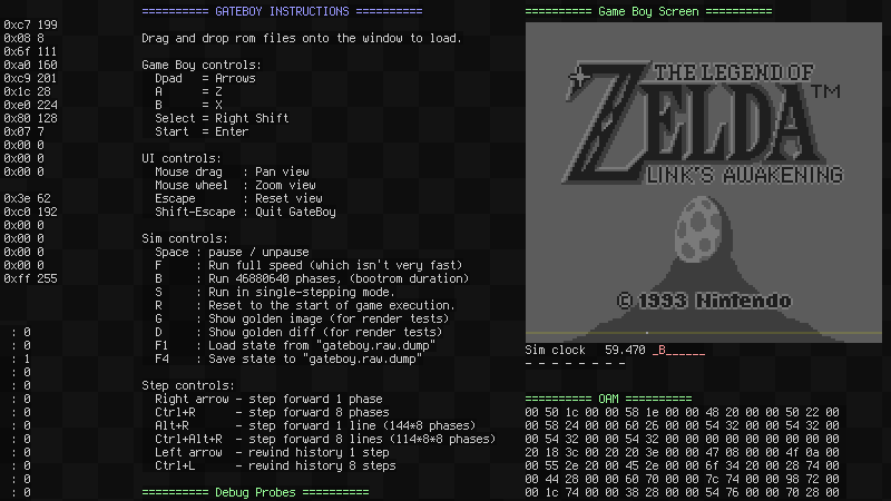
GateBoy is a project to emulate the Game Boy logic gate by logic gate. It’s a lower level approach that builds upon earlier work [Austin] did on a project called MetroBoy, which we featured previously.
The emulator was created by painstakingly reverse-engineering the logic of the Game Boy. This was done by poring over die shots of the actual DMG-01 CPU silicon. GateBoy emulates most of the chip, though avoids the audio hardware at this stage.
Presently, GateBoy runs at roughly 6-8 frames per second on a modern 4GHz CPU. As it turns out, emulating all those gates and the various clock phases at play in the DMG-01 takes plenty of processing power. However, compilation optimizations do a lot of heavy lifting, so in some regards, GateBoy runs impressively quickly for what it is.
[Austin] still has plenty of work to do before GateBoy is completely operational, and there are some strange quirks of the Game Boy hardware that still need to be figured out. Regardless, it’s a fantastic academic exercise and a noble effort indeed. Meanwhile, you might like to check out the Game Boy emulator that runs just one single game.


Hi, author here, happy to answer questions.
Also, please try out the Plait graph visualizer included in the repo. It’s a hacky mess, but you might have fun with it. :D
Extremely nice work getting to gate level. How low do you want to go?
http://www.visual6502.org/
https://sourceforge.net/projects/dice/
https://github.com/SourMesen/VisualNes
http://blog.visual6502.org/2014/10/atari-2600-simulation.html
Nobody that I know of has any quantum / atomic level emulation where we are doing anything remotely close to an atom by atom basis at this time. Even for an Atari, let alone even earlier than that.
The VisualNES alone typically runs at something about 1/1000th of the speed of a real NES. On modern hardware.
I think a NES simualtor should be doable at gate level, especially if the die’s already been reverse engineered. Any console past that generation probably isn’t feasible.
GateBoy will eventually have a “visual” mode, assuming I can parse the cell locations out of the .SVG that contains all the die annotations. I’d also like to add a logic visualizer to Plait, so you can run the sim and see gates in the schematic blnk.
Wow, that must have been a lot of work. So, as I understand it, every transistor that is not part of the audio circuitry or CPU was manually tracked in the die shots and it’s connections written down, is that right?
The CPU core emulation follows a more traditional emulation approach then?
How is the behavior of the emulator compared against real hardware? Is there some kind of custom board to upload programs and monitor the state of every cpu pin? When you get down to that level of accuracy even verifying the behavior is correct becomes a big problem.
It is awesome to see someone working on improving gameboy emulation at this level! While gameboy might be one of the best documented and most emulated systems out there, we still don’t have any “perfectly accurate” emulator and it looks like this yours comes very close.
Also, out of curiosity, do you have any estimates on how long this project took you?
A heck of a lot of work, yes. Furrtek did the initial schematic and die traces, though they had to make educated guesses as to what some of the gates did. Since they didn’t have a way to error check anything, the schematics have quite a few errors.
I re-traced a bunch of the cells and was able to work out definitively what they did via a sort of logic-Sudoku, and then I could write automated tests to verify that my solutions were correct.
My CPU emulator is a guess based on some constraints put on the bus behaviour by the rest of the chip – we know that the CPU must put a read request on the bus on phase X, if it’s a read from the cartridge then signal Y also has to be set, etcetera. It is simulated phase-by-phase, but not gate-by-gate.
Testing on real hardware is just a matter of writing some Game Boy assembly language and uploading it to a flash cart – Gekkio designed a flash cart that’s great for that purpose. You can also desolder the chip and put it on a breakout board for more serious testing, but I haven’t needed to do that yet – probing the LCD connector and the cartridge connector with a logic analyzer has been sufficient.
It’s been about two years of off-and-on work, both helped and hindered by lockdown and Covid.
I spent way too much time going down the rabbit hole that you’ve been digging. Thank you for such a thorough explanation, it’s a joy getting to come along with you on the adventure!
When are you throwing it on an FPGA?
The plan is to keep rewriting/refactoring GateBoy into higher levels of abstraction – LogicBoy will keep the registers but change the boolean logic to regular C expressions, MetroBoy will consolidate multiple 1-bit registers into regular C types.
Once that’s done, I am working on a tool that will mechanically translate the codebase into SystemVerilog for use on a FPGA. I’ve already done a proof-of-concept of the whole cycle (gates -> logic -> code -> verilog) with regression testing for a very small piece of the die, so I am confident that this will work out in the end. It’s gonna be another year or two before it’s all ready, though.
-Austin
Bravo. Need to comment how brilliant you guys are . I can understand enough in your comment to know how crazy awesome that is!!
Will you be targeting MiSTer for this?
They’ve already got good GameBoy cores, but wrapping a FPGA-enabled GateBoy in something that MiSTer can use would be reasonable.
When this was discussed on Hacker News, it was brought up that some aspects of the Game Boy are either sensitive to timing or can otherwise be considered analog in such a way that pure logic gates don’t capture. Someone mentioned that there’s not necessarily a single “correct” implementation for those parts of the design as they fluctuate between design revisions, batches, and even from unit to unit. That sounds like a real nightmare.
[Austin], can you talk more about which parts of the Game Boy are sensitive to these sorts of issues and how you’re approaching those parts of the Game Boy in Gateboy?
The glitches are generally a result of feeding unstable logic into a latch.
Unstable logic: Suppose I have an NOR gate and I feed it (0,1) – it outputs 0 – and then I feed it (1,0). You would expect the gate to continuously output 0, but you’d be wrong – if the second input arrives later than the first, there’s a tiny window of time where the output goes to 1.
Latches: A latch is like a light switch – push it up and it stays up, push it down and it stays down. Latches don’t have clock inputs, they switch whenever they see a “set” or “reset” signal… which also means that they respond to tiny glitch inputs like the 1 in the NOR example above.
I count 14 latches in the current simulation, with a variety of different gate configurations driving them. Eventually I’ll audit them all and figure out what else might be glitchy.
This is absolutely insane in an amazing way. It never seizes to astound me how much sheer interest and motivation is able to produce. Hats off to you Austin (and Furrtek of course), for an amazing amount of work and a _really_ cool proof of concept. The amount of work this has taken is just not commercially achievable, so the fact that this is done on your own time and motivation is astounding.
This is also the first real proof of concept of a full (bar the audio, but I’m mostly interested in the chip level ISR implementation that’s working) CPU reconstructed from die shots I’ve seen. I’m very curious if the fact that it’s now proven possible will lead to more research and tools for this way of emulation.
Really cool to see, I’ll definitely keep following the project!
Thanks for the compliments, it’s always nice to hear that people understand and appreciate the work.
“will lead to more research and tools for this way of emulation.”
That’s literally my end goal for GateBoy and the offshoots – I want a new and better way of writing hardware than Verilog/VHDL + proprietary packages like Vivado.
I want to be able to write a hardware simulation in C++, have my compiler verify that it can be correctly be implemented in hardware, and then run + debug the simulation using my normal C++ tools while also compiling to hardware for when I want to run the sim really really fast.
I don’t understand the work but I am enjoying reading about it :). Thanks for doing the work and documenting it so well.
Two of the links in the article point to the same URL.
Thanks, fixed.
For some reason comments didn’t show up for me on this article until 9 pm PST. I’m replying to them now.
an older system like atari 2600 wouldnt be easier to make this kind of logic gate reconstruction?
Probably, but I like the Game Boy more. :)
Any plans to turn this into a set of discrete 7400-series ICs? Not entirely a serious question, but it seems like it would be the next logic-gate step. And it has me wondering how quickly such a monstrosity would run.
you joke, but somebody made this thing – https://monster6502.com/
Can someone please help me understand the difference between this and something like a core for an FPGA?
You can write an FPGA gameboy core simply by looking at what goes in and out of the machine…you end up with a behavioral model of operation that can be exceedingly accurate and fast and it can all run at 4 (or 8 Mhz)…the process is very similar to classic emulation but a lot of the timing issues are easier to deal with.
This is approach is much different…this is like taking a brain scan of a worm and wiring up all the nerves as you see them and then getting worm like behavior out simulating how nerves work….its really cool stuff.
Honestly I get the feeling I need to read more about how FPGAs work to understand this all better. Your explanation helps, but I definitely need to work on understanding the details better.
I’m still learning baby’s first Arduino stuff, so I’m more than a little out of my depth here.