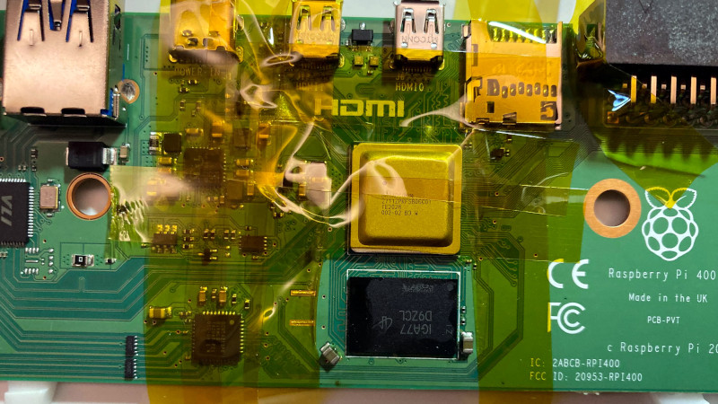
The all-in-one Raspberry Pi 400 computer is a capable device, but those seeking its maximum power may be disappointed by its 4 GB of memory. When the Pi 4 and Compute Module 4 have double that figure, surely the Pi 400 could catch up! A reddit user called [Pi800] rose to the challenge by replacing the 4 GB chip from the Pi 400 with the 8 GB chip from a Pi Compute Module, resulting in the so-called Pi 800, a working 8 GB all-in-one Pi.
As a piece of work it’s a deceptively straightforward yet extremely fiddly piece of soldering that requires a steady hand for even the most skilled of solderers. What takes it beyond the norm though is the reballing process. A ball-grid-array chip has a grid of small balls of solder on its underside that make the contacts, and these melt when it is soldered so require replacement before reworking. This is normally done with a template of carefully aligned holes to line up balls of solder in a stream of hot air, but lacking the template in this case the job was done by hand, laboriously ball by ball. A soldering task we’d hesitate to take on ourselves, so we’re impressed.
The result is an 8 GB all-in-one Pi, and it’s honestly not beyond the realms of possibility that an official version of this mod could be a future Raspberry Pi product. Perhaps we’ll wait for that, but should you be impatient then at least it’s possible to roll your own. It’s certainly not the first BGA memory swap we’ve brought you.


Mb and not GB?
Thanks. Fixed.
4 Mb as in four megabits?
4 megaballs, for the BGA
This guy gets it!
B^)
I dread the future where such BGA chips actually exist.
Just think of laying that out in a schematics! It will be pages on pager on pages with break out blocks for all the connections…. (And yes, schematics, not board layout. Laying out boards is fun in comparison.)
But just for fun.
A chip with 4 million pins in an array would be 2k x 2k pins. With a pin spacing of 0.05mm, it would be 10 cm wide. Even AMD’s EPYC processors would look small in comparison, and they have a much less dense land grid array. Though having 4000+ pins.
2000×2000 or 2048×2048?
It’s almost 5% difference.
“k” = 1000
“ki” = 1024 (However, few uses this in practice.)
However, outside the realm of RAM memory and CPU address space, using the 1024 scale is quite rare. Since not even everything in the computer world uses it, HDDs/SSDs use multiples of 1000, bus speeds typically do it too.
Alexander Wikström: which would be nice if there was widespread adherence to this convention. Which there really isn’t. When was the last time you saw DRAM modules specified in GiB?
BrightBlueJim I hope you noticed how even my own comment already states that it is rare and generally only applicable in a handful of areas. And even then it isn’t commonly used.
I were more pointing out the fact that one shouldn’t in general confuse the prefix “k” for 1024. (unless it is one of the exceptionally few cases where it might be the thing specified, but here any serious author should use “ki” instead. (listing specs on a product however rarely does this since people genereally don’t care about such trivialities. Even if HDD/SSD makers use 1000, while customers often unknowingly expect 1024 and complain that their new 1TB drive only has 931.32 GiB. (Though, most OSes writes “GB” when they should write “GiB”, though some seem to actually measure with 1000 instead.)))
In the end, getting everyone to switch over to Ki, Mi, Gi, Ti etc for when the 1024 scale is used is likely not a realistic expectation. But the 1024 scale is as stated not remotely common and only a programmer would think of 1024 before 1000 when seeing just “k”.
You joke, but who knows how far these will go in the future.
High-speed serial links seems to be where it’s headed.
If the footprint for eMMC is anything to go by, most of the pins will be not connected and just there for supporting some massive multi-chip-module.
Transputer lives!
HBM says otherwise. Very wide bus to save power. HBM2: 1024-bit wide per package
The problem with serial link is that your link needs to be high enough to carry the parallel data bit. If you need to carry 16-bit wide traffic then the *payload* part of the link need to run at 16X. The bleeding edge of GDDR and DDR are high enough to be a problem on PCB in parallel form. I don’t see them replaced with a serial link at x16 or x64 data rate.
> The bleeding edge of GDDR and DDR are high enough to be a problem on PCB in parallel form. I don’t see them replaced with a serial link at x16 or x64 data rate.
https://en.wikipedia.org/wiki/Compute_Express_Link
“CXL is built on the PCI Express (PCIe) physical and electrical interface with protocols in three areas: input/output (I/O), memory, and cache coherence.”
https://www.zdnet.com/article/samsung-develops-first-cxl-interface-based-dram/
For better or worse, Serial Attached Memory is coming.
Yes, that’s what’s written. That’s not what’s in the source (from an exceedingly brief glance) but that’s consistent throughout this article.
Wasn’t this just corrected in another post? My 200MHz Pentium I got used in 2001 to run Linux had 16 megs of RAM.
So isn’t this about gb?
As Jenny lives in England, I suspect it is SAE v. Metric problem.
B^)
Choose: SI v. SAE or imperial v. metric
Thanks to Brexit, Johnny Foreigner can keep his metres and kilogrammes. It’s furlongs and hogsheads from now on!
Indeed, our modeling application had FFF (Furlong Firkin Fortnight) units to appease the biblical-era old timers.
Because anything that can be corrected six times can be corrected seven: I think you probably mean 4 gigabytes, not 4 megabits. Orders of magnitude matter.
Yeah, there’s no way I would go through all that trouble for mere megabytes!
B^)
The new 8 GB memory BGA already has the fresh solder balls on it. No need to “reball”. Just clean the solder off the old pads and hot air that bad boy down with some flux.
But it is not new: salvaged fom a compute module
“As a piece of work it’s a deceptively straightforward yet extremely fiddly piece of soldering that requires a steady hand for even the most skilled of solderers. What takes it beyond the norm though is the reballing process.”
Great skills for becoming an iPhone screen replacer. ;-)
I’ve replaced more than a few screens, and I’ve never had to reball anything. Also, a steady hand is overrated if you’re good at working between heartbeats. =)
Well then let me introduce you to the iPhone 13! Replacing the screen now permanently bricks biometrics on the phone, and the only way to circumvent this is to snag a BGA chip from the old display module and put it on the new one. Wonderful, isn’t it?
Leave it to the youngsters. Yesterday I was having a bit of trouble with soldering a header (40 pins) unto my new RPI Zero 2 W board…. Eyes aren’t what they used to be! Nice job!
Oh and 8Gb would be nice on the 400, just because that is ‘intended’ for a desktop machine that may have lots of applications open at one time. All my other RPIs run headless, so, normally swimming in memory.
Wouldn’t it be simpler to skip the reballing and install a brand-new LPDDR3 chip? Surely the one pulled from the compute module is not anything specific to the Pi (they don’t have *that* large market share to have their own RAM chips made). Perhaps the chip shortages struck again…
But aligning the BGA balls manually is pure pain. The stencils are cheap and make the task 100x easier.
Also, it’s fortunate that the bootloader for the Pi does support a larger-than-official RAM size.
Think again. The zoro2W has rpi silicon with RAM. Anyway your conclusion may still be correct…
Why spend forever hand placing 100s of solder balls when reballing stencils are cheap and readily available? Rough example:
5 pcs 82801FBM BGA Reballing Stencil $7.95 USD
https://www.ebay.com/itm/233884882444
then it wouldn’t be on hackaday….
I didn’t know such a thing existed.
doh, it also didn’t reply to my rude post as I intended… ok, I’m logging off now. sorry everyone.
You’re killing me Clarance!!!!
its more like a Raspberry Pi 400+
but still missing a pcie switch ic, M2-NVME connector and a trap door =)
So it does work!
If they’d just release one with the 8GB I’d buy it straight away. Now I know there is no good reason it can’t be done
Here is a tutorial I found for the ram upgrade:
https://youtu.be/5pW4_nqcIWA