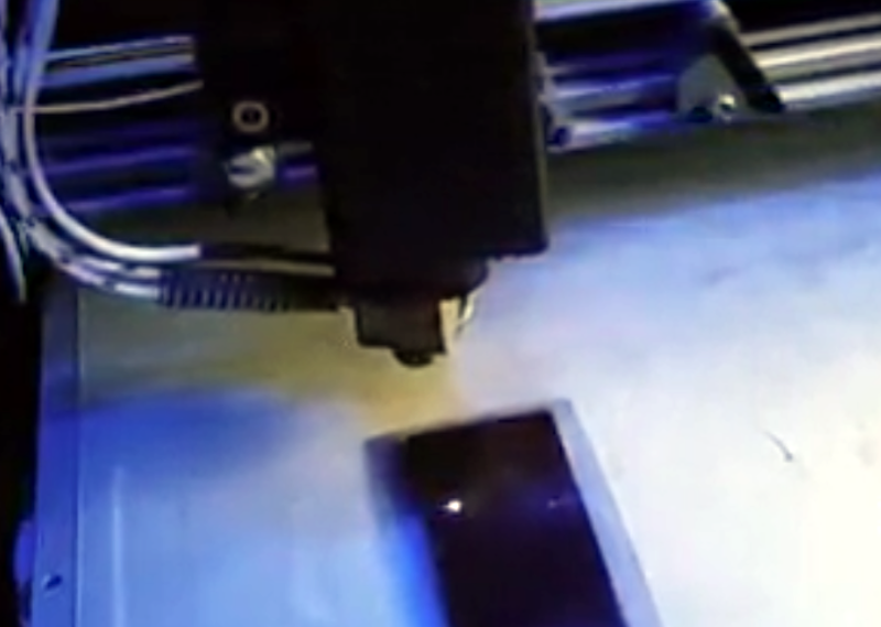
There are many ways to create printed circuit boards, but one of the more traditional ways involves using boards coated with photoresist and exposing the desired artwork on the board, usually with UV light. Then you develop the board like a photograph and etch it in acid. Where the photoresist stays, you’ll wind up with copper traces. Hackers have used lots of methods to get that artwork ranging from pen plotters to laser printers, but commercially a machine called a photoplotter created the artwork using a light and a piece of film. [JGJMatt] sort of rediscovered this idea by realizing that a cheap laser engraver could directly draw on the photoresist.
The laser dot is about 0.2 mm in diameter, so fine resolution boards are possible. If you have a laser cutter or engraver already, you have just about everything you need. If not, the lower-power laser modules are very affordable and you can mount one on a 3D printer. Most people are interested in using these to cut where higher power is a must, but for exposing photosensitive film, you don’t need much power. The 500 mW module used in the project costs about fifty bucks.
Of course, once you draw on the board with the laser, the rest of the process is like it always has been. Develop the board, etch, and all that. We wish the laser could drill the holes as that’s the part we hate the worst!
We’ve seen powerful lasers just cut boards, of course. You can also forego the photoresist and just let the laser burn off a coating of paint.


good luck doing a double sided board that way … alignment won´t be easy
i dont think alignment will be that hard. Just create a jig to hold it in place out of off cuts from other pcbs. Like we do with solder paste.
Been there, on a 3d printer. Other than figuring out how to get the two layers to align by using the 3d printer to use a Dremel to drill the 0.6mm VIAS, using G92 to zero the drag engraver to start the iso routing, I had a 3d printed board holder with 2 locations for 5mm socket head bolts. Next challenge was to arrest bed movement vs Y carriage movement between ISO routing the two layers. My bed was mounted to the carriage via long screws and springs. Typical for an i3 clone. Made brackets to allow bed leveling but arrest any other motion other than up/dn in relation to the Y carriage. Also needed to add a threaded rod diagonally to compensate for XY mechanical skew to get the tram equal.
End result after 2 months of ripped out hair and a few scrapped boards?
1 nearly perfect 14x14cm double sided PCB. Side to side via accuracy +/- 0.25mm across the whole board.
Just send your boards out.. they will be much better looking and you won’t have the non plated through hole soldering problem.
That is what fiducials are for.
Why always the nay saying. I made a PCB using a similar method, but by spray painting the blank PCB and using a diy scribe attached to my 3D printer. This scraped the paint off and the etch was successful. Even had vias as small as a 10th of an inch. Alignment is actually very easy if you know what you are doing. I will never go back to dry film again. I would be purchasing a laser to replace the scribe soon.
It’s more easy than you think. I often to make pcbs with home CNC laser. Two little holes and it’s perfectly alignable.
There is now open source / free software to control the type of fiber laser used in one of the linked articles: https://www.bryce.pw/engraver.html
These lasers are getting cheaper ($2200) though still a lot more expensive than a diode laser. The spot size is about a quarter of the resolution claimed in the article, nevermind the degradation from the theoretical resolution you get with etching. Etching is certainly doable for THT and low-density SMD, but for high resolutions it is hard to do repeatably without a fair bit of equipment.
Depends on etchant. I used to get very fine results with dilluted ferric chloride. 0402 pads could be done repeatedly, 0201 was becoming a hit-or-miss depending on quality of paper used, even toner made a difference as refills were more unpredictable.
a fiber laser engraver can blast the copper clean off…might need more passes, but it will do it…
Yup. It’s a misconception that 1064nm can’t machine copper. Even a 20W q-switched fiber laser can do it nicely. It does tend to lightly blacken the PCB, but most of that is just copper or copper oxide particles and much can be wiped away. The substrate remains nonconductive (as verified by my megaohmmeter at 500V)
For that, why not get a CNC and just mill the copper traces out?
The real issue is that regular dry film photoresist has a hard time going sub 85 ųm track/gap. There are a couple of solutions out there, but the material availability is prohibitive for DIYers. You also need to switch to a copper chloride etchant, dehydrate the photoresist post exposure, control the development cycle accurately, etc. I doubt it’s worth the effort to optimise the process at home. It took us several weeks to get it stable on professional equipment with high-quality film masks in a cleanroom. Once you go sub-100ųm dust, humidity and temperature swings become your enemies.
And anyway, illuminating PCBs directly with LDI systems is pretty standard in industry, contact lithography became exceedingly rare except for very large volumes or when pushing the edge of what’s possible. Of course the professional systems have more power and scan using an array of galvos.
I have used black paint sprayed onto the copper board and etched with my Ortur laser and the results are stellar. Quick chemical etch with muriatic acid/ Hydogen peroxide bath for just a few minutes. Done!
As an added note, my Ortur laser was under $500 and is a great machine with a large bed (approx. 24 x 24). See how I vent my machine out a basement window via 4 small holes in window frame. https://youtu.be/zGxicmPcgAc
I’ve made program which directly converts Gerber to GCODE.
https://github.com/korneliuszo/g2gv2
I think it will work in this application
Looks good. :-)
The only tiny problem is that it works slowly. But it’s not fatal.
Thank you.
HD projector and print the entire pcb in one go?
Two, and print both sides at the same time! Maybe use two laptop screens and sandwich your pre-sensitized board between them?
Nope. You need a resolution of 300 dpi or better for a decent PCB. Also photoresist wants 400 nm light with substantial power. And of course, the image must be perfectly focused and distortion-free. Now guess why advanced hobbyists still make contact copies with an old-fashioned UV lightbox…
400nm back lights behind the LCDs (remove the reflective layer) and image them onto the surfaces of the board.
https://youtu.be/VIiDLfR7loA
Lots of such videos on the tube. It is amazing how many solutions people have thought up for diy pcb
This will only work with very crude PCB designs, scattered light in the LCD’s front glass will blur the shadow. Useless for tiny stuff like MSOP-10 with 0.5 mm pitch. With the classic contact printing method there is no such scattering, because the ink or emulsion side of the mask is in direct contact with the photoresist.
UV resin printer for the resist?
“The laser dot is about 0.2 mm in diameter, so fine resolution boards are possible.”
This of course presumes that the etching process will be perfect which it never is.
Alignment is actually very easy and Spot on, even for 0.3mm drills.
I built this here some years ago and still use it quite often:
https://youtu.be/Dj59uGOOX4g
Just my Version makes 0.1mm tracks consistently good :-)
Have you tried making a pcb inductor?
Perhaps you could try stacking bifilar coils in an alternating stack of pancakes? So each layer also tries to counter it’s own self capacitance. I’ve always wanted to try that with copper wire, but I’ve never had the funding or patience. It seems like a 0.1mm track could in theory make that a lot easier.
Vladimir Trondin’s build using a polygon mirror LSU from a Samsung laser printer – easy to build as you only need a single moving axis and no backlash issues to deal with as the axis always moves
in a single direction.
https://youtu.be/zA2SxA9U4ys
Andry Black published an opensource Raspberry PI + STM32 based high speed
laser PCB exposer similar to Alphacrow’s HLDI which uses the guts of an inkjet printer including
the high res optical encoder tape which inkjets use.
https://youtu.be/Fx7F5YykWQc
https://easyeda.com/andryblack
https://github.com/andryblack/pcb-printer-host
https://github.com/andryblack/pcb-printer-firmware
Also a nice solution. I know a few guys that built this 7 years ago and this inspired me. They had issues getting the focus equal over the full with as the lens Was not made for Blue Light. Anyway, for small Boards this is no issue.
I’d like to look into reusing LCDs and UV sources from SLA Printers.
I might try multi-layer PCB process with a similar technique. I’m still fighting layer alignment better than +/- 0.25mm and cannot through plate holes. Problem is, hard to beat OSH or PCB-way.
None of them provide half an hour delivery. That’s where you beat them.
That is the conundrum these days. Professionally made boards are cheap, but you may have to wait 2 or 3 weeks. I have actually never had a need for a printed circuit board “now”, and if I need it now, I perfboard, breadboard or “dead-bug” or something like that, and use it until the nicely made boards come in. I have made single layer boards for fun, and have used them in permanent projects, but have not really ever found it necessary, as my time to make one from scratch is often worth more than just buying nice ones and waiting while I do other things.
Yah ive always felt that if you actually NEED it NOW, something went terribly wrong in your planning process. Lean that lesson the hard way, move on, and plan better in the future.
I tried the same with K40 laser cutter, but it didn’t work out.
Even at the lowest power level at which it would lase it was too powerful and would burn the resist instead of exposing it. I guess being IR means exposing wouldn’t really work in any case. Normal developer did nothing but fortunately the burned resist dissolved in isopropyl alcohol faster than the unexposed resist.
But fine resolution was not possible because the burned edges were kind of flaky. Here is a PCB with 0.5 mm pitch IC and 0603 passives: http://jpa.kapsi.fi/stuff/pix/k40_pcb1.jpg
And for comparison here is a PCB made with transparency film and traditional exposure, but same etching process: http://jpa.kapsi.fi/stuff/pix/valotus_pcb.jpg
Black spray paint works fine as an etch resist that can be removed by a K40 or most other laser cutters.
Any PCB technology that can’t make a 2-layer board with vias is frivolous. The simplest Chinese Arduino board has vias.
Oh, ok.. This individual seems to think that there is no use for single sided boards. Meh.
Plenty of youtubes about using a laser to develop photoresist.
https://www.youtube.com/results?search_query=laser+pcb
I have not seen them all, but I did see the one from Marco Reps and that was quite a good one.
Anyone thought of using a resin 3D printer display to expose the PCB? The resolution is about 60um and is using UV light.
Yes, this approach could work.
Incidentally I found that “cooking” the resist works almost as well, though not as reliable if you keep the board at a controlled (low) temperature it can work to prevent blurring and resulting low resolution.
Active cooling with a Peltier can be effective here and ensure repeatability.
For something like this it doesn’t matter what the wavelength is, the side emission from a 445 or 450nm laser is more than enough and only needs <30mW so a PL450 will do at a pinch if focused well to ensure a minute spot.
These aren't cheap but filtering is comparatively simple, and an OD5.5+ (red pass) goggles set with additional measures like running it in a light tight box and use of a CMOS camera + remote display will ensure a margin of safety.
I found that the sort of diodes used in PS3 or HD-DVD modules DO work but only if you use parts from the sled itself, such as the waveshape plate mounted in low melting point alloy to clean up the beam.
Why not:
Print artwork on laser printer compatible transparency sheet
Position over sensitized PCB
Expose with DIY UV LED array, or a cheap UV (finger)nail lamp
I’ve got one of the $70 (years ago) 1W laser engravers typically of the NEJE “brand” (with many clones) which uses CD-ROM laser transport mechanisms for laser movement (which is why they were so cheap). I’d like to avoid the need for photosensitive resist entirely and have considered burning off a thin, flat black lacquer coating on a PCB instead. Anyone tried that?
Not with a 1W diode laser but it works great with black spray paint and a K40 CO2 laser on low power. I imagine it would work with most diode laser cutters.
Couldn’t you just put the board covered with photoresist on the bed of a resin printer (without resin !) to expose it
I’ve always wondered if you could make circular PCBs with an unmodified DVD burner using custom software, anyone ever looked into it?
You mean like the old Lightscribe drives that were briefly a thing?
Interesting idea.
Have a somewhat damaged but working LS drive (busted sled) here, so a minimal modification should do it.
Incidentally, the biggest problem with these is bypassing the eject signal, so the resulting image can be etched multiple times.
Yes you can use a LS CD-R as a negative, though again there are faster ways to do this.