It’s a pity that more electronics enthusiasts haven’t taken the hobby to its ultimate level: making your own semiconductors. There are plenty of good reasons for that: chief among them is the huge expense involved in obtaining the necessary equipment. But for the sufficiently clever, there are ways around that.
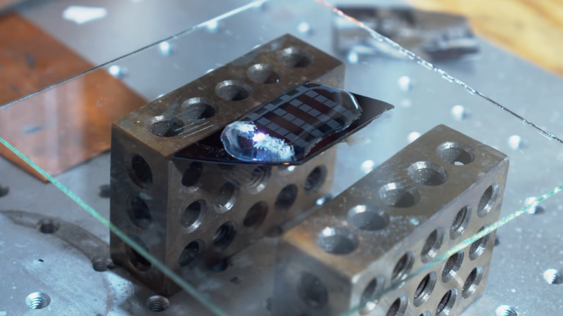
[Zachary Tong] is dipping his toes into the DIY semiconductor world, and further to the goal of keeping costs to a hobbyist scale, is experimenting with laser doping of silicon. Doping is the process of adding impurities to silicon wafers in a controlled manner to alter the electrical properties of the semiconductor. [Zach]’s doping method is a more localized version of the simple thermal diffusion method, which drives a dopant like phosphorus into silicon using high temperatures, but instead of using a tube furnace, he’s using a fiber laser.
The video below shows his two-step process, which first blasts the silicon oxide layer off the wafer before doping with the laser shining through a bath of phosphoric acid. The process is admittedly fussy, and the results were mixed at best. [Zach]’s testing seems to suggest that some doping occurred, and it even looks like he managed to make something reasonably diode-like using the method.
Although the jury is still out on [Zach]’s method, we thought the effort was the important bit here. Granted, not everyone has a fiber laser kicking around to replicate his results, but it’s always good to see progress in the DIY semiconductor field. Here’s hoping [Zach]’s work, along with the stuff that [Sam Zeloof] is doing, kicks off a spate of garage semiconductor fabs.
Thanks to [BaldPower] for the tip!


Would it be possible to use this technology to use laser doping to etch a diffraction grating for photonic experimens?
I’m specifically interested in trying to make a 0.3 µm filter for UV light, for disinfection purposes (for the reason why, look up visualcapitalist Zooming In: Visualizing the Relative Size of Particles)
The hypothesis is that resonance will cause the particles to dance, and shatter into smaller pieces, increasing their entropy such that they won’t reform within human timescales.
Any ideas about where to get access to a scanning electron microscope would also be much appreciated!
The lowest you can go with structuring is the wavelength. Look up LIPS (laser induced periodic surface structures). With a 1064nm laser this is about 1000 lines/mm, but there will be a lot of other periodic structures on the surface so a proper, useable grating is not possible. :/
I never get tired of surprising these homemade silicon chips.
The knowledge curve is unfortunately still very high, I hope someday we will have something like local “printers/manufacturers” (similar to space makers), where you can come up with a chip idea and come out of it with a working prototype.
Before they talk, I know a lot to do with FPGA, but I mean something more universal in electronics, not just logic.
SMT components are almost small enough already. So I’m sure we’ll get there soon.
Hmm interesting idea that actually, the smallest end of SMT are so damn tiny simpler ‘IC’ could be fabricated entirely from them in a reasonable footprint, though I expect same as all the home brew silicon we have seen the end result wouldn’t be particularly efficient or effective compared to the existing general purpose ICs or FPGA.
Still being your own verified ‘silicon’ gives it merits in security and would be a good learning experience.
Looking forward to these homebrew processes getting sophisticated enough to make a modern 6502 equivalent.
(Regarding the opening line) I know what they mean, and while this is now true, it was once common for hobbyists to construct semiconductor diodes from galena crystals. I’ve also seen point contact transistors here before (this one made from a mass-produced diode): https://hackaday.com/2010/11/05/making-point-contact-transistors/ Making more advanced constructs without corporate backing is definitely a noteworthy feat.
Why not use an ion beam? Seems like an easier task than using photons to push it in thermally. Let the dopant do all the work…